International Journal of Mining, Materials, and Metallurgical Engineering (IJMMME)
ISSN: 2562-4571

Volume 9 - Year 2023 - Pages 30-36
DOI: 10.11159.ijmmme.2023.005
Low Temperature TSV Interconnection with Ultra-thin Ag Nano-twinned Films Sputtered on Si Wafers for 3D-IC Advanced Packages
Yin-Hsuan Chen1, Yen-Ting Chen1,Tung-Han Chuang *1,2
1National Taiwan University, Department of Material Science and Engineering
106 Taipei, Taiwan.
sammichen8815@gmail.com; a5331812@gamil.com
1Ag Materials Technology Co., AMTC, Hsinchu Science Park, 30078 Hsinchu, Taiwan.
*Corresponding author: tunghan@ntu.edu.tw
Abstract - Nanotwinned structure has been attracting a great deal of attention due to their excellent mechanical and electrical properties. In this study, ultra-thin nanotwinned Ag films can be fabricated by DC magnetron sputtering with moderate substrate bias. Within these nanotwinned films, only 100-400 nm thick equiaxed-grin transition layer was formed between the nanotwinned region and Si substrate observed by Focused ion Beam (FIB). For the analysis of nanotwinned films, the as-deposited films are shown to have a strong (111) preferred orientation. The roughness of the films was observed below 10 nm, which was smooth enough and acceptable for metal direct bonding. Ag-to-Ag direct bonding was then performed to satisfy the requirement of TSV interconnections. The ultra-thin nanotwinned Ag films with (111) preferred orientation will have many potential applications in interconnects and 3D IC packaging.
Keywords: Nanotwins, thin film, TSV interconnection, 3D-IC, packaging.
© Copyright 2023 Authors This is an Open Access article published under the Creative Commons Attribution License terms. Unrestricted use, distribution, and reproduction in any medium are permitted, provided the original work is properly cited.
Date Received: 2023-11-08
Date Revised: 2023-11-24
Date Accepted: 2023-12-05
Date Published: 2023-12-13
1. Introduction
As the transistors reach atomic scale and fabrication costs continue to increase, Moore’s law is approaching its limit. The technique of three-dimensional integrated circuits (3D IC) is one of the promising solutions to the problem. One of the 3D IC packaging technologies is 3DFabric™ of TSMC, including SoIC® (System-on-Integrated-Chips), CoWoS® (Chip-On-Wafer-On-Substrate), and InFO (Integrated Fan-out). The main principle of 3DFabric™ focuses on stacking the dies, leading to high-density and compact packaging. SoIC® refers to a type of wafer-on-wafer bonding technique that integrates both homogeneous and heterogeneous chips into a SoC (System-on-Chips) system, resulting in a thinner profile, bigger bandgap, lower loss, and better power integrity and signal integrity. CoWoS® utilizes silicon interposers and microbump to integrate several chips, forming CoW. Through silicon via is revealed by chemical mechanical polishing and the packaging size is reduced by redistribution layer and bonding with the substrate with C4 bump. InFO can be divided into InFO_PoP(Integrated Fan-out Package-on-Package) and InFO_oS(Integrated Fan-out on Substrate). InFO_PoP has a high density of redistribution layer and through InFO via, smaller size and better electrical and thermal properties due to the lack of organic substrate and C4 bump. In addition, the density of the redistribution layer in InFO_oS is even higher. InFO features substrate-less packaging, thus decreasing the vertical height, the distance to the heat sink, and the thermal shock.
Miniaturization of the electronic components requires the stacking of heterogeneous materials. Creating a robust bonding interface by low-temperature bonding approaches that can prevent thermal damage and withstand high service temperature is the key to successfully fabricating such electronic devices. Various techniques have been applied for low-temperature direct bonding.
Solder bonding depends on the chemical reaction between the solder and the bonding metal by heating. This method provides the advantages of low cost, low fabrication temperature, and high reliability. Moreover, the characteristic of self-alignment and the ability to rework of Pb-Sn solder system allows a wide variety of applications in the flip-chip process. However, one of the notable drawbacks is the intermetallic formed in the bonding interface can easily cause brittle fracture and failure and can also cause thermal, electrical, and mechanical problems in the joint [1]. The addition of flux is also undesirable.
Eutectic bonding is a bonding technique that bonds materials together using two or more elements with its eutectic composition. The eutectic temperature is typically much lower than the melting point of a pure element, the bonding process can be applied at low temperatures. Au-Si is the most established system of eutectic bonding, with a eutectic temperature of 363℃. The melting temperature reduced dramatically from 1063℃ at pure gold [2][3]. Wang et al. have performed eutectic bonding with the Au-Sn system at temperatures below 300℃ for hermetic sealing [4]. An average thickness of less than 1.5 µm of the Au-Sn layer was used to perform the eutectic bonding process, which can reach an average shear strength of approximately 23 MPa [5]. However, failure occurred due to the stress produced during the bonding process by the mismatch of the thermal expansion coefficients between the die and the bonding layer [6].
Solid-liquid interdiffusion (SLID) bonding can form a high-quality bond at low temperatures that can also withstand temperatures higher than its formation temperature, which provides outstanding thermal performance [7]. The diffusion between high-melting metal and low-melting interlayer forms intermetallic compounds (IMCs) in the joint. By controlling the characteristics of the interlayer and heating rate, a void-free bonding interface can be obtained. The bonding interface creates hermetic sealing in low temperatures, which is ideal for applications in harsh environments. Several systems were used in SLID bonding including Au-In, Au-Sn, Ag-In, Ag-Sn, and Cu-Sn [7-10].
Thermo-compression bonding is referred to as solid-state bonding. The diffusion of elements between metal and metal is driven by the heat and pressure applied on the bonding interface. However, oxidation of the metal interface can often weaken the reliability of the bond. Preventing oxidation or removing the oxide formed in the bonding interface can successfully improve the bond quality and mechanical strength.
In the method of surface activated (SAB) bonding, an ion beam with inert gas was used to etch the substrate to remove the surface contaminant. The clean surface provided stronger bondability, and covalent or metallic bonds formed when the surfaces are bought into contact. It can be performed at room temperature without any heat treatment, resulting in no thermal damage or residual thermal stress in the joint, and also prevent doping of impurities and defects generation. However, it is unable to bond dielectric materials such as glass, silicon oxide, and sapphire. Also, since the surface condition of the specimen is critical, the process has to be performed in an ultrahigh vacuum [11-13]. Surface activated bonding of Si and SiO2 by argon beam at room temperature possessed strength equally with the sample bonding by conventional bonding process at 1100℃ [11]. Thin Cu film was bonded directly together at room temperature by the SAB method activated with an argon ion beam of 40-100 eV [12].
To accomplish the interconnection of TSV, several methods had been applied. It is revealed that surface activated bonding method can directly bond silicon wafers with Cu-Cu bonding at room temperature [12][13]. However, it is not practical due to its high processing cost and time. Interestingly, Cu nanotwinned films have a highly (111) preferred orientation, resulting in a higher atomic diffusivity [14][15]. Thus, low-temperature Cu-Cu direct bonding becomes more practical, which is also one of the solutions for fine-pitch microbumps for 3D IC packaging. According to Chen et al., the direct bonding temperature of electroplating Cu nanotwinned films can be decreased to 150°C for 60 min, which is lower than the reflow temperature of 250°C for Pb-free solders. The high temperature may trigger thermal mismatch whenever the coefficient of thermal expansion of the silicon wafer and the other material has a large difference. In addition, few voids were found in the surface between a Cu thin film with (111)-oriented nanotwinned structure and a randomly-oriented Cu film, which is attributed to the 3-4 orders higher diffusivity of Cu atoms on (111) surfaces than other planes [16]. Further, a highly (111)-oriented Cu nanotwinned film possesses the lowest oxidation rate compared to other surfaces [17]. In fact, highly (111)-textured Ag nanotwinned films deposited with magnetron sputtering process can also achieve low-temperature Cu-Cu direct bonding, which can be directly bonded at 150°C for 1h and 10 min at 250 °C [18]. Chang et al. further showed that highly (111)-oriented nanotwinned Ag films can achieve metal bonding under an air atmosphere of 190/200°C in 3 min [19]. Since highly (111)-oriented nanotwinned films satisfy metal direct bonding, the method of fabricating high-quality thin nanotwinned films becomes a critical issue. The morphology of nanotwinned film includes a columnar crystal region that contains high-density nanotwins near the surface and a randomly oriented equiaxed-grain region, as known as the transition layer, which is formed between the substrate and the nanotwin region. The existence of transition layer was attributed to the lattice mismatch of the nanotwin region and the substrate. Thus, the high-quality nanotwinned films should possess a smaller transition layer and a large columnar crystal region.
There are two major fabrications of high-density nanotwinned films so far, including electroplating and magnetron sputtering. For the electrodeposited Cu nanotwinned films, dense columnar nanotwinned films were formed by using the sputtered Cu seed layer with strong (111)-orientation. On the other hand, the transition layer was larger without the highly oriented seed layer [20]. Apart from the seed layer, applied reverse current can also improve the quality of nanotwinned films. Reverse current affected the grain size and surface roughness, and it remarkably retard the formation of the transition layer [21]. Further, the selective dissolution behavior of reverse current causes non (111)-oriented grains to be dissolved earlier than (111)-oriented grains due to their higher surface energy, which facilitates the formation of the columnar nanotwinned Cu microstructure [22]. For the magnetron-sputtered nanotwinned films, it is revealed that the existence of the adhesive layer can effectively improve the quality of nanotwinned films. It is proved that the Ti adhesive layer not only enhances the bonding strength between the nanotwinned film and Si substrate but also reduces the lattice mismatch for the epitaxial growth of nanotwinned Ag films on Si substrates as well as the proportion of transition layer. In addition, the film with a thinner transition layer tends to possess better thermal stability, which is attributed to the fact that there would be fewer random grains replacing the nanotwinned structure, especially at high temperatures [23][24]. Moreover, applying negative bias voltages during sputtering can facilitate the formation of dense nanotwinned columnar structures, lower the transition layer thickness, enhance (111) texture, and increase indentation hardness due to the Ar+ ion bombardment effect [25]. While the fabrication and the quality of Cu nanotwinned films can be optimized, Cu-Cu direct bonding at low temperatures is also improved, boosting the performance of backside metallization for power devices.
The interconnection for CoWoS and WoW requires film thickness lower than 1 µm for optimal performance. Therefore, it is necessary to develop a reliable process to fabricate sub-micron thickness nanotwinned films. With moderate substrate bias, the ultra-thin Ag and Cu nanotwinned films with strong (111) surface orientation can be fabricated for metal direct bonding applications such as the 3D IC advance package.
2. Experimantal
In this work, thin nanotwinned films were fabricated by a DC magnetron sputtering system (JUBSUN TECH, SGS-500). The sputtering chamber was evacuated to a base pressure < 5×10^(-6)Torr (6×10^(-4) Pa). High purity (99.9995%) Argon gas was used and maintained at 5 mTorr (0.67Pa). Before the coating process, Si substrates were ultrasonically cleaned in acetone and deionized water subsequently to promote the adhesion of films. In addition, the substrates were pre-sputtered by argon discharge at a bias of -500 V for 30 min to remove the surface oxide layer. For the coating process, the thickness of 100 nm Ti adhesive layer was first deposited onto Si substrates before sputtering the Ag thin films. The sputtering power of Ti and Ag were all 150 w and the deposition rate was 0.1 nm/s and 0.895 nm/s, respectively. The deposition temperature varies from room temperature to 50°C. The holder was fixed at 10 rpm. After deposition, the bonding process was performed. The samples were cut into 4 × 4 mm2 pieces. Next, the Ag films were placed face to face and bonded at 200°C at a bonding pressure of 20 Mpa for 60 min.
The samples were analyzed by a focused ion beam (FIB, Hitachi NX2000) to observe the microstructure and determine the film thickness. Orientation maps, crystallographic textures, and grain boundaries of nt-Ag films were analyzed using electron backscattered diffraction (EBSD, JEOL JSM-7800F). The data were analyzed using OIM software, and the proportion of grains with (111) orientation was calculated with a misorientation threshold of 15˚. X-ray diffraction (XRD, Rigaku TTRAX) was used to determine the texture of the as-deposited nanotwinned Ag films. The surface roughness (Ra) of the thin film surfaces was measured with an atomic force microscope (AFM, Burker Dimension Edge). FIB was also used to examine the bonding interface condition and the microstructure arrangement of the Ag nanotwinned film.
3. Results and Discussions
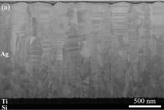
The cross-sectional metallography of Ag films with a thickness of 1.5μm and 700nm sputtered on Si (100) wafer with pre-coatings of 100nm Ti thin film are shown in Figure 1. The substrate bias applied to these two Ag films with different thicknesses was -150V and -250V, respectively. The results indicated that many Ag columnar grains grew normally to the Si substrate and a high density of nanotwins piled up on one another was observed in both cases. Upon comparing the microstructures of the two nanotwinned Ag films, Figure 1(a) reveals that the transition region, consisting of random grains, has a thickness of approximately 0.4±0.02 μm. Notably, this thickness exceeds that of the Ag thin film subjected to a -250V substrate bias, as illustrated in Figure 1(b), which measures approximately 0.1±0.01 μm. The results implied that applying an appropriate substrate bias during the sputtering process can effectively reduce the thickness of the transition layer and promote the formation of nanotwinned columnar grain structures. In the previous study, many methods were used to reduce the thickness of the transition layer, such as adding a buffer layer or seed layer. In our work, ultra-thin nanotwinned Ag film can be fabricated by sputtering with substrate bias, allowing the potential application of 3D-IC advanced packaging.

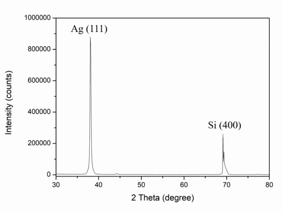
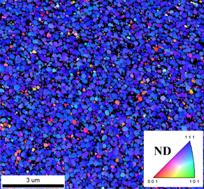
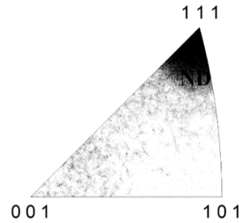
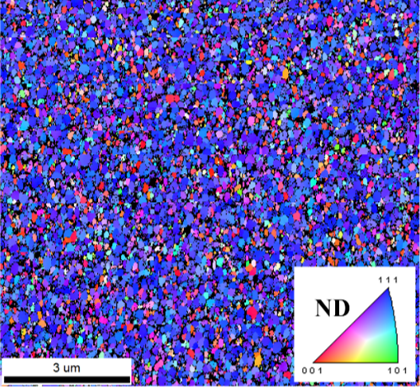
The XRD spectrum depicts the grain orientation of the sputtered Ag film with -250V substrate bias. As shown in Figure 2, the Ag thin film presented strong (111) peak intensity with Si (400) peak. Furthermore, the proportion of (111) orientation of the Ag films was identified by top-view EBSD with a scanning step size of 28nm. As shown in Figure 3 and 4, both nanotwinned Ag thin films exhibited a strongly preferential (111) orientation. The inverse pole figure maps showed the proportions of (111) orientation grain was measured to be 71% and 93%, respectively. In addition, the proportion of Σ3 coincidence twin boundaries to the total grain boundaries was 25% and 54%, respectively. These results demonstrated that the (111)-oriented Ag thin film contained high-density twin boundaries.
For the low-temperature bonding application, one of the critical demands is the fast diffusion path of the highly (111)-preferred surface of the sputtered nanotwinned Ag thin film. The (111) is the closest-packed plane in FCC metals and has the fastest surface diffusivity among all the other crystalline planes. The surface diffusion rate of the (111) plane can be 3 to 4 orders of magnitude higher than those of other crystal planes, such as (110) and (100). This fact indicates that, if the ratio of (111)-oriented grains is enhanced on the bonding surface, the diffusion rate can be increased substantially, which will allow the bonding process to occur at low temperatures for 3D-IC packaging.
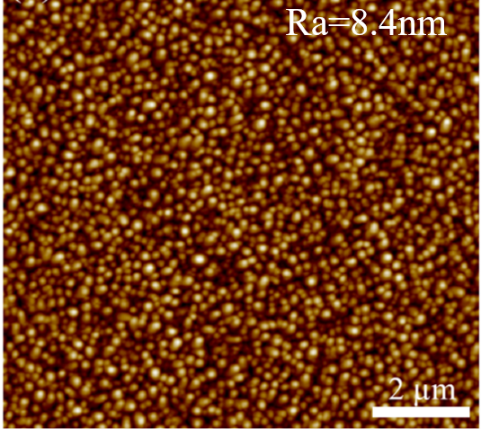
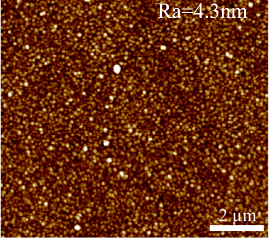
For bonding applications, it is known that surface roughness also plays a critical role to affect bonding quality. In Figure 5 and 6, the surface roughness of the Ag film with 1.5 μm and 700 nm was identified by AFM. The Ra values of the Ag surface were 8.4 nm and 4.3 nm, respectively. These results showed that the thinner nanotwinned Ag film has smaller surface roughness and these values are similar to the electroplated (111) nt-Cu with CMP reported by Lin [27]. Furthermore, silver is softer and less prone to oxidation than copper, making it suitable for low-temperature direct bonding.

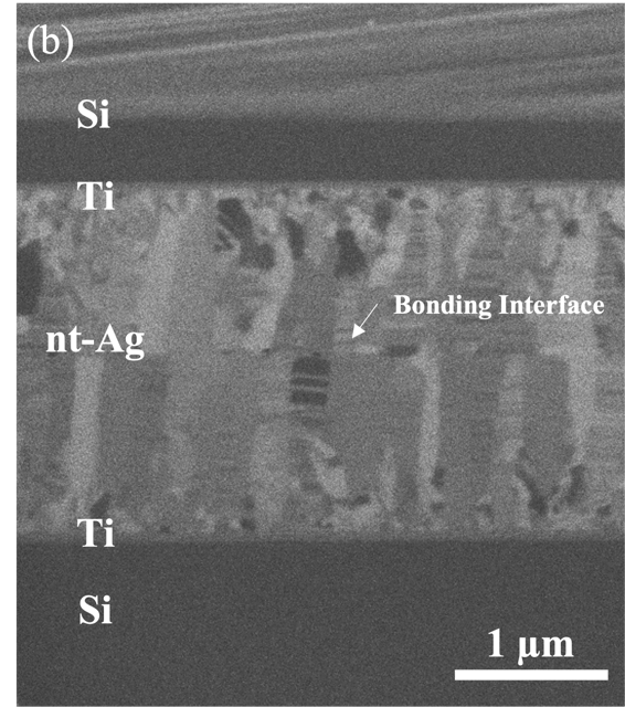
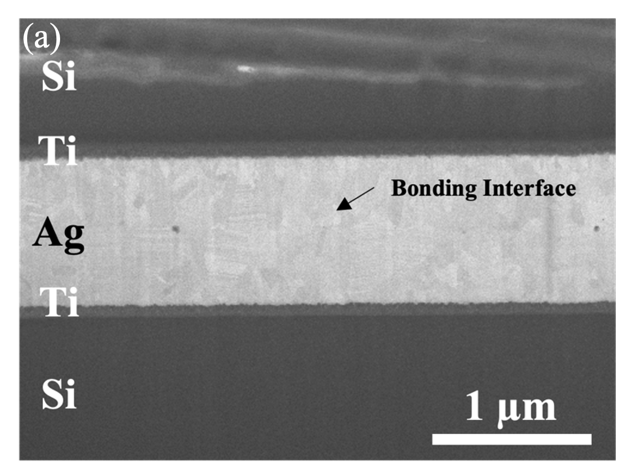
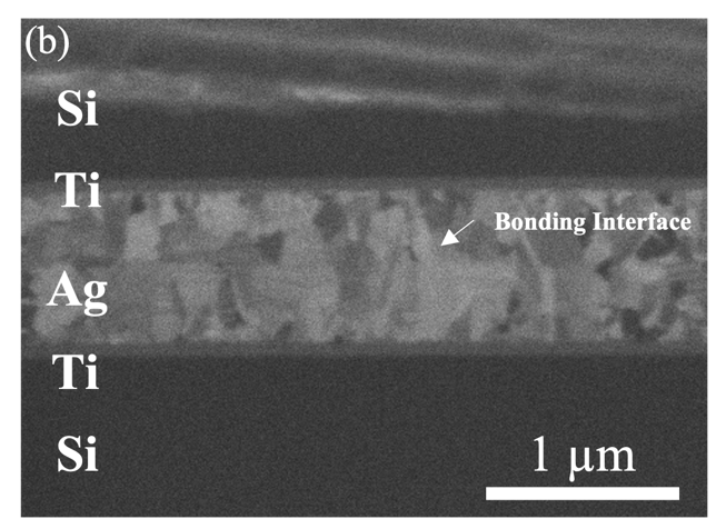
The cross-sectional FIB electron beam images and ion beam images of the bonding samples of 700nm and 1.5µm-thick Ag film were shown in Figure 7 and 8. After bonding at 200℃ for 60 minutes under 20 MPa, it can be observed in the electron beam images that only a few voids appeared in the bonding interface of both samples, indicating that the fast diffusion path of (111)-oriented nanotwinned structure is helpful for low-temperature direct bonding. Ion beam image also revealed the nanotwinned structure of Ag films remains stable without obvious grain growth after the heating of the bonding process, which resulted from the excellent thermal stability of nanotwins.

4. Conclusion
In this study, 1.5 μm and 700 nm-thick Ag films with strong (111) orientation and high-density nanotwinned structure were successfully fabricated by using DC magnetron sputtering process with moderate substrate biases. FIB analyses provided good agreements for the enhancement effect of Ar+ ion bombardment on the formation of the nanotwinned structure and decreasing the thickness of the transition layer. XRD and EBSD results confirm that the surface has a strong (111)-preferred orientation. The surface roughness (Ra values) of Ag films is lower than 10nm. With the aid of the fast diffusion path on (111) planes and low surface roughness, Ag-Ag direct bonding can be achieved at 200°C for 60 min under 20 Mpa in a regular vacuum of 1×10⁻³ torr. This approach provides a potential solution for interconnects and 3D IC packaging.
Acknowledgement
This study was sponsored by the Emerging Technology Application Program of the Hsinchu Science Park R & D program of Ag Materials Technology Co., LTD under Grant No. 112AO03A.
References
[1] Matijasevic, G. S., Wang, C. Y., & Lee, C. C. (1993). Thermal stress considerations in die-attachment. Thermal Stress and Strain in Microelectronics Packaging, 194-220. View Article
[2] Lin, Y. C., Baum, M., Haubold, M., Fromel, J., Wiemer, M., Gessner, T., & Esashi, M. (2009, June). Development and evaluation of AuSi eutectic wafer bonding. In TRANSDUCERS 2009-2009 International Solid-State Sensors, Actuators and Microsystems Conference (pp. 244-247). IEEE. View Article
[3] Wolffenbuttel, R. F., & Wise, K. D. (1994). Low-temperature silicon wafer-to-wafer bonding using gold at eutectic temperature. Sensors and Actuators A: Physical, 43(1-3), 223-229. View Article
[4] Wang, Q., Choa, S. H., Kim, W., Hwang, J., Ham, S., & Moon, C. (2006). Application of Au-Sn eutectic bonding in hermetic radio-frequency microelectromechanical system wafer level packaging. Journal of electronic materials, 35, 425-432. View Article
[5] Demir, E. C., Torunbalci, M. M., Donmez, I., Kalay, Y. E., & Akin, T. (2014, December). Fabrication and characterization of gold-tin eutectic bonding for hermetic packaging of MEMS devices. In 2014 IEEE 16th Electronics Packaging Technology Conference (EPTC) (pp. 241-245). IEEE. View Article
[6] Sun, L., Chen, M. H., Zhang, L., He, P., & Xie, L. S. (2020). Recent progress in SLID bonding in novel 3D-IC technologies. Journal of Alloys and Compounds, 818, 152825. View Article
[7] Sun, L., Chen, M. H., Zhang, L., He, P., & Xie, L. S. (2020). Recent progress in SLID bonding in novel 3D-IC technologies. Journal of Alloys and Compounds, 818, 152825. View Article
[8] Bernstein, L. (1966). Semiconductor Joining by the Solid‐Liquid‐Interdiffusion (SLID) Process: I. The Systems Ag‐In, Au‐In, and Cu‐In. Journal of the Electrochemical Society, 113(12), 1282. View Article
[9] Tollefsen, T. A., Larsson, A., Taklo, M. M. V., Neels, A., Maeder, X., Høydalsvik, K., ... & Aasmundtveit, K. (2013). Au-Sn SLID bonding: A reliable HT interconnect and die attach technology. Metallurgical and Materials Transactions B, 44, 406-413. View Article
[10] Tollefsen, T. A., Larsson, A., Løvvik, O. M., & Aasmundtveit, K. E. (2013). High temperature interconnect and die attach technology: Au–Sn SLID bonding. IEEE Transactions on Components, Packaging and Manufacturing Technology, 3(6), 904-914. View Article
[11] Takagi, H., Maeda, R., Chung, T. R., & Suga, T. (1998). Low-temperature direct bonding of silicon and silicon dioxide by the surface activation method. Sensors and Actuators A: Physical, 70(1-2), 164-170. View Article
[12] Takagi, H., Kikuchi, K., Maeda, R., Chung, T. R., & Suga, T. (1996). Surface activated bonding of silicon wafers at room temperature. Applied physics letters, 68(16), 2222-2224 View Article
[13] Kim, T. H., Howlader, M. M. R., Itoh, T., & Suga, T. (2003). Room temperature Cu–Cu direct bonding using surface activated bonding method. Journal of Vacuum Science & Technology A: Vacuum, Surfaces, and Films, 21(2), 449-453. View Article[14] Agrawal, P. M., Rice, B. M., & Thompson, D. L. (2002). Predicting trends in rate parameters for self-diffusion on FCC metal surfaces. Surface Science, 515(1), 21-35. View Article
[15] Liao, C. N., Lu, Y. C., & Xu, D. (2013). Modulation of crystallographic texture and twinning structure of Cu nanowires by electrodeposition. Journal of the Electrochemical Society, 160(6), D207. View Article
[16] Chen, C., Liu, C. M., Lin, H. W., Huang, Y. S., Chu, Y. C., Lyu, D. R., ... & Tu, K. N. (2016, January). Low-temperature and low-pressure direct copper-to-copper bonding by highly (111)-oriented nanotwinned Cu. In 2016 Pan Pacific View Article
[17] Zhou, G., & Yang, J. C. (2005). Initial oxidation kinetics of Cu (100),(110), and (111) thin films investigated by in situ ultra-high-vacuum transmission electron microscopy. Journal of Materials Research, 20(7), 1684-1694. View Article
[18] Lai, Y. C., Wu, P. C., & Chuang, T. H. (2021). Characterization of interfacial structure for low-temperature direct bonding of Si substrates sputtered with Ag nanotwinned films. Materials Characterization, 175, 111060. View Article
[19] Chang, L. P., Wang, J. J., Hung, T. H., Chen, K. N., & Ouyang, F. Y. (2022). Direct metal bonding using nanotwinned Ag films with (1 1 1) surface orientation under air atmosphere for heterogeneous integration. Applied Surface Science, 576, 151845. View Article
[20] Liu, C. M., Lin, H. W., Lu, C. L., & Chen, C. (2014). Effect of grain orientations of Cu seed layers on the growth of< 111>-oriented nanotwinned Cu. Scientific reports, 4(1), 1-4. View Article
[21] Chen, K. J., Wu, J. A., & Chen, C. (2020). Effect of Reverse Currents during Electroplating on the⟨ 111⟩-Oriented and Nanotwinned Columnar Grain Growth of Copper Films. Crystal Growth & Design, 20(6), 3834-3841. View Article
[22] Kim, M. J., Lim, T., Park, K. J., Cho, S. K., Kim, S. K., & Kim, J. J. (2012). Characteristics of pulse-reverse electrodeposited Cu thin films: I. effects of the anodic step in the absence of an organic additive. Journal of The Electrochemical Society, 159(9), D538. View Article
[23] Lai, Y. C., Wu, P. C., & Chuang, T. H. (2021). Thermal stability of grain structure for Ag nanotwinned films sputtered with substrate bias. Materialia, 20, 101215. View Article
[24] Liu, C. M., Lin, H. W., Huang, Y. S., Chu, Y. C., Chen, C., Lyu, D. R., ... & Tu, K. N. (2015). Low-temperature direct copper-to-copper bonding enabled by creep on (111) surfaces of nanotwinned Cu. Scientific reports, 5(1), 1-11.] View Article
[25] Wu, PC., Lai, YC. & Chuang, TH. Enhancing effect of substrate bias on nanotwin formation of sputtered Ag thin films. J Mater Sci: Mater Electron 32, 21966–21973 (2021). View Article
[26] Z. Cui, K. Han, Y. Xin, D.R. Waryoba, A.L. Mbaruku. Highly textured and twinned Cu films fabricated by pulsed electrodeposition, Acta Mater. 55 (2007) 4 429–4 438. View Article
[27] Lin, P. F., Tran, D. P., Liu, H. C., Li, Y. Y., & Chen, C. (2022). Interfacial characterization of low-temperature Cu-to-Cu direct bonding with chemical mechanical planarized nanotwinned Cu films. Materials, 15(3), 937. View Article