International Journal of Mining, Materials, and Metallurgical Engineering (IJMMME)
ISSN: 2562-4571

Volume 9 - Year 2023 - Pages 37-44
DOI: 10.11159.ijmmme.2023.006
Low Temperature Direct Bonding of Ge Chips with DBC Alumina Substrates using Ag Nanotwinned Films
Yen-Ting Chen1, Yin-Hsuan Chen1, and Tung-Han Chuang*1,2
1Institute of Materials Science and Engineering, National Taiwan University, 106 Taipei, Taiwan.
2Ag Materials Technology Co., LTD, Hsinchu Science Park, 30078 Hsinchu, Taiwan.
a5331812@gmail.com ; sammichen8815@gmail.com ; tunghan@ntu.edu.tw
*Corresponding author: tunghan@ntu.edu.tw
Abstract - Epitaxial Ag nanotwinned films with highly (111)-preferred orientation were deposited by magnetron sputtering onto germanium substrates, some with the addition of a Ti layer and application of negative substrate bias. A high density of Ag nanotwins with an average twin spacing of 2.18 nm formed in the Ag columnar structures. Twin boundaries formed along the direction perpendicular to the growth direction of the film. The influences of the Ti interlayer and negative substrate bias on the formation of Ag nanotwins were also examined. The highly (111)-textured thin films had an impressive film surface roughness, as low as 11.2 nm. The (111)-oriented nanotwins provided higher surface diffusivity than did other orientations. The electrical resistivity decreased significantly as more (111)-oriented nanotwinned structures formed. The bonding experiment was also performed at 200℃ for 60 min at a bonding pressure of 20 MPa, and extremely rare voids appeared at the bonding interface. The combination of low surface roughness, rapid diffusivity on the (111)-planes, and lower electrical resistivity present a high possibility of reliable interconnections for future microelectronic technology via direct bonding.
Keywords: (111)-oriented Ag nanotwin; Ti interlayer; Negative substrate bias; Ge substrates.
© Copyright 2023 Authors This is an Open Access article published under the Creative Commons Attribution License terms. Unrestricted use, distribution, and reproduction in any medium are permitted, provided the original work is properly cited.
Date Received: 2023-11-05
Date Revised: 2023-11-22
Date Accepted: 2023-12-03
Date Published: 2023-12-21
1. Introduction
Germanium (Ge) was once the major substrate material used in the early days of semiconductor transistor and integrated circuit (IC) technology. However, it was later completely replaced by silicon (Si) due to the higher thermal stability of silicon at high temperatures and relatively low cost. Despite the fact that the application of Ge substrates for electronic devices is far less developed than that of Si, Ge is still an attractive material for both n-type and p-type field-effect transistors (FETs) due to its high electron and hole mobility, which are about 2 times higher for electrons and 4 times higher for holes than those of Si [1]. Nevertheless, many researchers have reported on the superior properties of Ge substrates. Sircar et al. described the electron transport properties of Ge substrates with epitaxial p-type GeMn thin films, which gives rise to an effective 2- layer conduction scheme [2].
Uchida et al. also proposed using the decreased thermal transport properties of Ge substrates deposited with Al2O3 insulator films to minimize the damage by Joule heating in Ge-based Metal-Oxide-Semiconductor Field-Effect Transistor (MOSFET) devices [3]. As Ge has irreplaceable merits, especially for high speed and/or low-power applications, research attempts continue with the aim of achieving high-performance Ge-based devices [4].
Due to the lack of a stable Ge native oxide and its much lower melting temperature than that of Si, Ge usually exhibits inferior thermal stability and can only be used at significantly lower temperatures. The limited operation temperature range of Ge restricts its application to device components where it is advantageous, rather than for all purposes. Recent progress towards metallization on ever-smaller devices has focused attention on thin film technologies due to the rapidly evolving discipline of nanotechnology. Several metal deposition techniques on Ge substrates have been successfully implemented to improve the performance of Ge-based devices; however, most of them require high growth temperatures, which are inapplicable to standard semiconductor technology [5]. Porter et al. deposited nanostructured noble metal films on Ge by electroless deposition via galvanic displacement reaction of Ge with gold (Au), palladium (Pd) and platinum (Pt) salts [6]. However, in Westmacott et al.’s work, it was found that only face-centered cubic (FCC) metals such as aluminum (Al), silver (Ag) and gold (Au) formed epitaxial films directly on the (111), (110) and (100) surfaces of Ge substrates due to the binary eutectic relationships of the FCC metals that formed with Ge. The epitaxial relationships of the metal films highly depend on the crystallographic factors for metal–metal epitaxy and on the substrate surface structure for metal–semiconductor epitaxy [7].
Since their first discovery, studies on FCC nanotwinned structures have never ended, especially those on Cu thin films. Cu thin films with highly nanotwinned structures have demonstrated impressive electrical, thermal and mechanical properties [8-16]. The nanotwinned structures consist of large amounts of coherent ∑3 (111) twin boundaries, which have much lower energy than high angle grain boundaries and hence will be much more stable at higher temperatures [17]. Interestingly, twinning in Ag has received little attention, as compared with that in Cu. Ag is known for having the lowest stacking fault energy among all elemental FCC metals; in other words, Ag might form even higher densities of nanotwins than the other FCC metals. Ag also has excellent electrical and thermal conductivity at room temperature, so its use in microelectronics applications is quite common. To satisfy the demand for increasing integration density on IC chips, the continuous scaling down of the pitch and size of IC interconnections is necessary. As a result, the traditional flip chip process leads to more reliability issues due to high working temperatures, intermetallic compounds (IMCs) and voiding issues. Recently, direct bonding methods have attracted much interest in the semiconductor industry [18]. The formation of direct metal-to-metal joints is assisted by pressure and temperature, and to form high quality joints, the requirements for surface roughness and vacuum are stringent. Another factor is that Ag is much softer than Cu, so a lower bonding pressure is required. Employing Ag as the bonding layer may also negate the risk of die cracking caused by the high bonding pressure. Our recent studies have developed a method of Ag–Ag direct bonding via the highly (111)-oriented Ag nanotwinned films, with sound joint quality [19]. The high density of CTBs formed in the Ag nanotwinned films increases the rate of surface diffusion, resulting in reductions in bonding temperature and time. We believe that this bonding technique is valuable for die attachment for power devices as it causes minimum heat damage to the chips and substrates.
In this paper, we report the comprehensive characterization of Ag nanotwinned films sputtered on (111) Ge. We show herein the effects of the Ti adhesion layer on the epitaxial growth, morphology and texture of the Ag nanotwinned films. The effect of negative substrate bias is also discussed. Finally, we propose an approach for fabricating efficient interconnections in Ge-based electronic devices via low-temperature direct bonding of Ag nanotwinned films.
2. Experimental
Ag thin films of 4 µm thickness were grown on single-crystal (111) Ge by magnetron sputtering in a vacuum chamber with a base pressure (under Ar atmosphere) of 0.67 Pa (5 mTorr) and about 6 × 10⁻⁴ Pa (5 × 10⁻⁶ Torr) during deposition. The substrates were deposited either with or without a Ti adhesion layer for examination of the effects of the adhesion layer on the epitaxial growth of Ag nanotwinned films on Ge substrates. In addition, negative bias was applied to some of the substrates for examination of the effect. The target source was high purity (99.99%) Ag. To obtain epitaxial growth of the thin films, substrates with well-defined surfaces were required. Prior to deposition, the Ge substrate surfaces were polished mechanically until smooth. The substrates were further treated with plasma cleaning of negative bias of 500V for 30 minutes to remove the oxide layer from the substrate surfaces. The deposition rate was kept constant at about 0.85 nm/s for Ag and 0.1 nm/s for Ti, under sputtering power of 150 W. After deposition, the specimens were examined using a PANalytical-X’Pert PRO to identify the grain orientation of the Ag films. TEM cross-section samples were prepared using focused ion beam (FIB) milling integrated in an FIB-SEM, a Hitachi NX2000. The SEM imaging of the cross section was performed to obtain the metallographic observations of the Ag films. The determination of the transition layer thickness involved measuring the distance from the Ag/Ge or Ag/Ti boundary to the deposition front of the grown Ag random grains at 10 equidistant points on the FIB micrograph and subsequently calculating the average thickness. The standard deviation for the various transition layers ranged between 0.15 and 0.29 μm.
Transmission Electron Microscopy (TEM) bright-field images were acquired using a FEI Tecnai G2 F20 operated at 30 kV to observe the cross-sectional microstructure of the Ag nanotwinned films. Atomic Force Microscopy (AFM) measurements were performed using a Burker Dimension Edge AFM. Electron backscatter diffraction (EBSD) was performed with a JEOL JSM-7800F to identify the crystal orientations and twin densities of the samples. The planar and cross-sectional patterns were analyzed in OIM TSL analysis software, including the proportion of (111) crystal grain orientations and Σ3 coincident grain boundaries within the nanotwin thin film. The computation of coincident site lattice grain boundaries as a ratio to the total grain boundaries was conducted with a permissible tolerance angle of 15 degrees. Furthermore, indentation hardness was measured with a Hysitron TI 980 TriboIndenter. The electrical resistivity is measured by four-point probe.
3. Results and Discussions
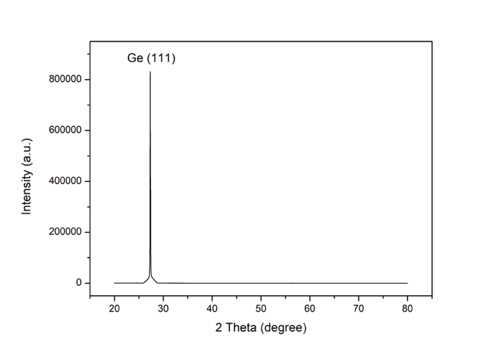
The structural properties of the single-crystalline (111) Ge substrates were first examined by XRD analysis. Figure 1 presents the XRD spectra of the Ge substrates before they were sputtered with the Ag nanotwinned film. The XRD analysis identified a strong Ge (111) peak, suggesting the high purity of the single crystal structure.
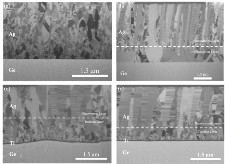
To observe the effects of both the Ti adhesive layer and negative bias on the Ag nanotwinned films, the thickness of the Ag of all four specimens was kept the same. The cross-sectional FIB metallography in Figure 2 revealed the crystal structure of the Ag thin films. As shown in Figure 2, an equiaxed-grain transition layer formed between the Ag nanotwinned region and the substrate surface. Nanotwinned structures are well-known to have excellent mechanical properties, as they maintain high mechanical strength without compromise to the high ductility of the materials. Thus, the transition layer could act as the weakest point and degrade the regularity of the Ag nanotwinned films. Therefore, it is essential to eliminate the transition layer if Ag films are to be further adopted as reliable interconnections.
The FIB cross-sectional ion images also indicated that the addition of the Ti adhesive layer and negative substrate bias both had profound impacts on the grain size and thickness of the transition layer. Fig 2a showed the ion image of the direct-coated Ag film without negative substrate bias. Few twins formed in the coarse grain of the Ag thin film, but the twin density is relatively low. Also, the columnar structure of nanotwins is not observed, which indicated that there is almost no nanotwinned structure when fabricated without a Ti adhesive layer and negative substrate bias. As shown in Figure 2b, the direct-coated Ag film with negative substrate bias had a relatively thick transition layer (1.32 µm) with large grains that formed within, whereas the Ti-precoated Ag film without negative substrate bias in Figure 2c possessed a thinner transition layer (1.08 µm) and much finer equiaxed grains. But part of the thin film showed a non-nanotwinned structure that grew to the surface of the Ag thin film. Figure 2d shows that, when both a pre-coated Ti layer and negative bias were applied to the substrate, the result was an optimized nanotwinned structure with a relatively thinner transition layer (0.61 µm) having a fined-grain structure.
The Ag nanotwinned layer was continuous over the Ti layer, indicating that the Ti was responsible for a decrease in surface energy and thus acted as an adhesion layer between the substrates and the Ag films. The smaller grain size in the transition layer was attributed to the enhanced adhesion of the deposited Ag provided by the Ti adhesion layer. According to the previous literature, the enhanced wetting behavior of the adhesion layer by various types of metal seeding could increase the nucleation sites for the deposition of Ag, eventually leading to a much denser transition layer [20-22]. To further increase the density of nanotwins, we applied negative bias to the substrate. Our previous research suggested that kinetic energy of ion bombardment induced local stress distribution and defects that formed nanotwinned structure. The high strain rate of magnetron sputtering and high density of grain boundaries due to nanoscale grains also provide reasonable explanations to the formation of nanotwins. Therefore, it is possible that the nanotwinned structure formed to release the local stress during the fabrication of the Ag thin films [23].
To identify the crystal orientation of the Ag film in cross-section, EBSD analysis was used to analyze the crystal structure, crystallographic orientation and grain sizes of the Ag nanotwinned film. Both the cross-sectional and surface areas of the thin film were observed.
Figure 3a presents the cross-sectional EBSD analysis of the Ag thin film without the Ti adhesive layer and negative substrate bias. It is obvious that most of the grains were randomly oriented. Figure 3b shows the surface grain orientation; the result indicated that only 44% of the grains had (111)-orientation.
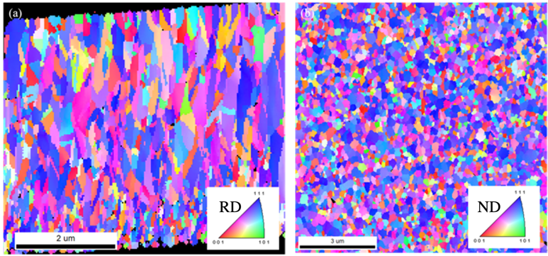
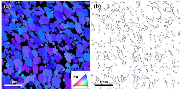
Increasing the amount of nanotwinned structures in Ag thin film by both adding a Ti adhesive layer and applying negative substrate bias resulted in the growth of more (111)-oriented grains, as shown in Figure 4 and Figure 5. In the inverse pole figure (IPF) in Figure 4a, the (111)-oriented Ag nanotwins mostly formed in the columnar structures within the nanotwinned region of the Ag film. The grains in the transition layer were randomly-oriented. Figure 4b shows only the (111)-orientation distribution (blue region) of the Ag film, confirming that Ag nanotwins only formed in the nanotwinned region. The grain size was ~0.12 ± 0.08 µm. Conversely, the fine grains at the transition layer were mostly randomly oriented. Moreover, the Σ3 and Σ9 twin boundary distributions, presented in Figure 4c, comprised 33.5% and 3.3% of all the grain boundaries, respectively.

As shown in Figure 5a, the surface grains exhibited the strong (111)- preferred orientation of the Ag nanotwinned film over about 74.1% of the surface, as indicated in blue in the plane-view EBSD IPF. Figure 5b presents the corresponding EBSD IPF map with the Σ3 and Σ9 twin boundary distributions on the Ag film surface. Note that the (111)-plane has the fastest surface diffusivity among all the planes of Ag, by about 4 to 5 orders of magnitude [24]. The high surface diffusivity of the Ag nanotwinned film facilitated the movement of Ag atoms along the (111)-plane and filled the voids at the bonding interface, which allowed successful direct bonding at lower temperatures.
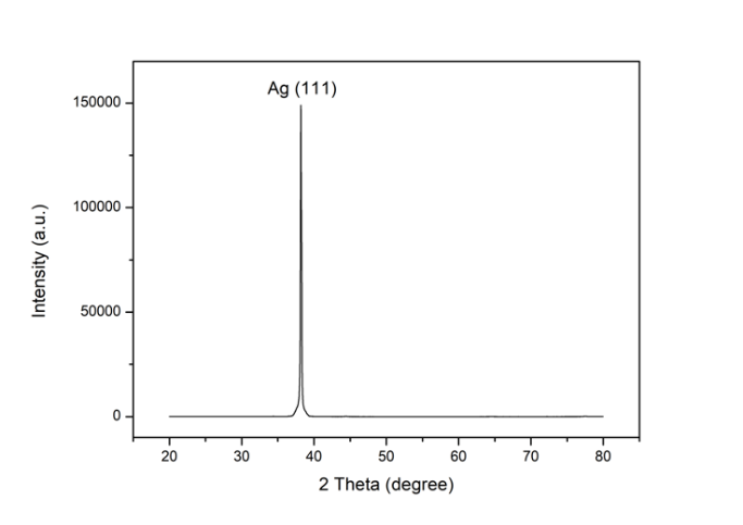
The XRD pattern in Figure 6 shows an intense Ag (111) peak almost without any other diffraction peaks. Consistent with the EBSD and FIB observations, the result indicated that high purity Ag (111) grains formed on the film. As clearly shown in the bright-field TEM cross-sections of the Ag nanotwinned film in Figure 7a, the Ag nanotwins were specifically structured in a lamellar arrangement within the columnar grains along the film growth direction. The Ag columnar structures had widths distributed from 100 nm to 200 nm. The ordered arrangement of the twin lamellae was essentially alternating twinning (Figure 7b), wherein each Ag atomic column has alternating Ag nanotwins along the [011] zone axis. The high density of Ag nanotwins introduced within the Ag columns by the released of stress that produced by ion bombardment resulted from the magnetron sputtering deposition. However, the formation mechanism of the nanotwins remains under debate. Ag is a typical FCC metal; its CTB usually have an asymmetrical tilt boundary of the ∑3 misorientation. Figure 7c indicated that the twins (T) and the matrix (M) are stacked alternatively, with the coherent twin boundary in between them. Also, a mirror symmetry relationship can be observed along the twin boundary. The average twin spacing was measured as 2.18 nm. Such a unique arrangement of the lamella provides multiple interfaces for surface diffusion, allowing bonding process to occur at relatively low temperatures.
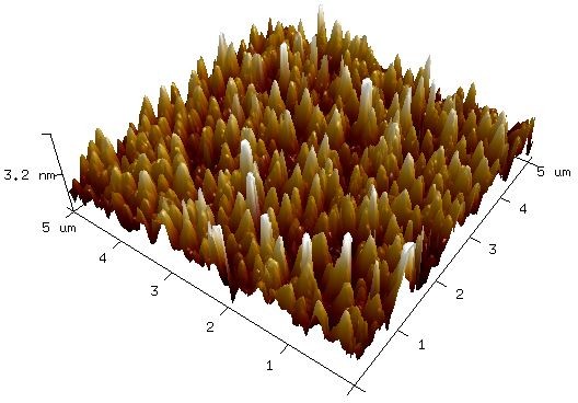
Both the effective surface diffusion and the area of contact at the bonding interface were used to describe the bondability of the Ag nanotwinned films. AFM observations with a scanning area of 5 × 5 µm2 showed the surface roughness (in Ra) of the direct sputtered Ag film to be 11.2 nm, which fulfilled the surface smoothness requirement for direct bonding. The substrate surface smoothness is one of the critical parameters that affects the surface roughness of the Ag nanotwinned film. During deposition, these columnar structures continued to grow; during this growth, the Ag nanotwins piled up on each other and eventually reached the film surface. The film growth would form numerous small bumps on the film surface, which would determine the surface roughness of the Ag films. This possibility was further confirmed by the 3D-AFM plot in Figure 8.

For applications in the semiconductor industry, it is also essential to evaluate the electrical properties. Nanotwins are well-known to have both low electrical resistivity and excellent mechanical properties. The electrical resistivity of the Ag nanotwinned films on Ge substrates was measured by four-point probe. When applying negative substrate bias, the electrical resistivity decreased from 2.773×10^(-8) (Ω∙m) to 2.013×10^(-8) (Ω∙m), indicating that the nanotwinned structure had a positive effect on electrical conduction. Also, the hardness of the Ag thin film increase from 0.85 GPa to 1.3 GPa with more portion of (111)-orientated nanotwins.
After fabrication of the highly (111)-preferred orientation nanotwins, the bonding experiment has been performed. The Ag thin film sputtered on the Ge substrate was bonded with a DBC substrate. The bonding process was performed at a low temperature of 200℃ for 60 min at a bonding pressure of 20 MPa and chamber vacuum of 10-3 torr. The FIB image of the bonded sample has been shown in Figure 9. It can be seen that virtually void-free interfaces can be achieved by employing Ag nanotwinned film sputtered on the Ti-precoated Ge single crystal. The densely-stacked nanotwinned columnar structure can also be observed in the FIB ion image in Figure 9. The results indicated that highly (111)-oriented Ag nanotwins have a positive effect on fast diffusion occurring in the bonding interface, which is a potential application of low-temperature direct bonding.

Conclusions
In this study, we have demonstrated the fabrication of Ag nanotwinned films with a (111)-preferred orientation deposited on (111) Ge substrates by magnetron sputtering. The experimental observations by FIB and TEM revealed that high portions of Ag nanotwins formed in the Ag columnar structures. It was also found that the portion of (111)-oriented nanotwins can be increased by the addition of a Ti adhesive layer. Moreover, applying negative substrate bias enhances the formation of nanotwinned structures, as indicated by the strain relaxation mechanism. EBSD analysis also showed that highly (111)-oriented grains formed, comprising about 37.9% of the cross-sectional grain structure and 74.1% of the surface region. High densities of coherent ∑3 and ∑9 twin boundaries also formed along with the Ag nanotwins during deposition. The XRD scan confirmed the strong (111)-preferred orientation of the Ag films, which provided rapid diffusion paths for surface diffusion. The electrical resistivity decreased by 27.4% due to the application of both the Ti adhesive layer and negative substrate bias. A direct bonding experiment was performed at 200℃ for 60 min at a bonding pressure of 20 MPa. The result showed only few voids in the bonding interface, which indicated that the achievement of low surface roughness and rapid diffusivity of the Ag film surface can reduce the bonding temperature and time required for direct bonding technology in advanced packaging interconnections.
Acknowledgement
This study was sponsored by the industrial and academic cooperation program of the Hsinchu Science Park R&D program of Ag Materials Technology Co., LTD. and the Ministry of Science and Technology, Taiwan, under Grant No. 109A18A.
References
[1] P. Hashemi, T. Ando, "SiGe Devices," in High Mobility Materials for CMOS Applications, Woodhead Publishing Series in Electronic and Optical Materials, 2018, pp. 205-229. View Article
[2] N. Sircar, S. Ahlers, C. Majer, G. Abstreiter, D. Bougeard, "Interplay between electrical transport properties of GeMn thin films and Ge susbtrates," Physical Review B, 83, pp. 125306, 2011. View Article
[3] N. Uchida, Y. Najajima, L. Bolotov, W. H. Chang, T. Maeda, Y. Ohishi, "Heat transport properties of alumina gate insulator films on Ge substrates fabricated by atomic layer deposition," Materials Science in Semiconductor Processing, vol. 121, pp. 105396, 2021. View Article
[4] A. Toriumi, T. Nishimura, "Germanium CMOS potential from material and process perspectives: Be more positive about germanium," Japanese Journal of Applied Physics, vol. 57, no. 1, pp. 010101, 2017. View Article
[5] G. Masini, L. Colace, G. Assanto, H. C. Luan, L. C. Kimerling, "High- Performance p-i-n Ge on Si Photodetectors for the Near Infrared: From Model to Demonstration," IEEE Transactions on Electron Devices, vol. 48, no. 6, pp. 1092-1096, 2001. View Article
[6] L. A. Porter, H. C. Choi, A. E. Ribbe, J. M. Buriak, "Controlled Electroless Deposition of Noble Metal Nanoparticle Films on Germanium Surfaces," Nano Letters, vol. 2, no. 10, pp. 1067-1071, 2002. View Article
[7] K. H. Westmacott, S. Hinderberger, U. Dahmen, "Physical vapour deposition growth and transmission electron microscopy characterization of epitaxial thin metal films on single-crystal Si and Ge substrates," Philosophical Magazine A, vol. 81, no. 6, pp. 1547-1578, 2001. View Article
[8] O. Anderoglu, A. Misra, F. Ronning, H. Wang, X. Zhang, "Plastic flow stability of nanotwinned Cu foils," International Journal of Plasticity, vol. 26, no. 6, pp. 875-886, 2010. View Article
[9] O. Anderoglu, A. Misra, H. Wang, F. Ronning, M. F. Hundley, X. Zhang, "Epitaxial nanotwinned Cu films with high strength and high conductivity," Applied Physics Letters, vol. 93, no. 8, pp. 83-108, 2008. View Article
[10] X. H. Chen, L. Lua, K. Lu, "Electrical resistivity of ultrafine-grained copper with nanoscale growth twins," Journal of Applied Physics, vol. 102, no. 8, pp. 083708, 2007. View Article
[11] O. Anderoglu, A. Misra, H. Wang, X. Zhang, "Thermal stability of sputtered Cu films with nanoscale growth twins," Journal of Applied Physics, vol. 103, no. 9, pp. 094322, 2008. View Article
[12] X. Zhang, A. Misra, H. Wang, J. G. Swadener, A. L. Lima, M. F. Hundley, R. G. Hoagland, "Thermal stability of sputter-deposited 330 austenitic stainless- steel thin films with nanoscale growth twins," Applied Physics Letters, vol. 87, no. 23, pp. 233116, 2005. View Article
[13] L. H. Xu, D. Xu, K. N. Tu, Y. Cai, N. Wang, P. Dixit, J. H. L. Pang, J. M. Miao, "Structure and migration of (112) step on (111) twin boundaries in nanocrystalline copper," Journal of Applied Physics, vol. 104, no. 11, pp. 113717, 2008. View Article
[14] K. Lu, L. Lu, S. Suresh, "Strengthening Materials by Engineering Coherent Internal Boundaries at the Nanoscale," Science, vol. 324, no. 5925, pp. 349-352, 2009. View Article
[16] X. W. Liu, L. G. Sun, L. L. Zhu, J. B. Liu, K. Lu, J. Lu, "High-order hierarchical nanotwins with superior strength and ductility," Acta Materialia, vol. 149, pp. 397-406, 2018. View Article
[17] Fullman, R. L. "Interfacial free energy of coherent twin boundaries in copper," Journal of Applied Physics, vol. 22, no. 4, pp. 448-455, 1951. View Article
[18] J. Q. Wu, C. C. Lee, "Low temperature Ag-Ag Direct Bonding Technology for Advanced Chip-Package Interconnection," IEEE 69th ECTC, 2019, pp. 2302-2308.
[19] Y. C. Lai, P. C. Wu, T. H. Chuang, "Characterization of interfacial structure for low-temperature direct bonding of Si substrates sputtered with Ag nanotwinned films," Materials Characterization, vol. 175, pp. 111060, 2021. View Article
[20] M. Todeschini, A. B. Silva Fanta, F. Jensen, J. B. Wagner, A. Han, "Influence of Ti and Cr Adhesion Layers on Ultrathin Au Films," ACS applied materials & interfaces, vol. 9, no. 42, pp. 37374-37385, 2017. View Article
[21] A. Anders, E. S. Byon, D. H. Kim, K. Fukuda, S. H. N. Lim, "Smoothing of ultrathin silver films by transition metal seeding," Solid State Communications, vol. 140, no. 5, pp. 225-229, 2006. View Article
[22] N. Formica, D. S. Ghosh, A. Carrilero, T. L. Chen, R. E. Simpson, V. Pruneri, "Ultrastable and Atomically Smooth Ultrathin Silver Films Grown on a Copper Seed Layer," ACS applied materials & interfaces, vol. 5, no. 8, pp. 3048-3053, 2013. View Article
[23] Wu, P. C., Lai, Y. C., & Chuang, T. H. "Enhancing effect of substrate bias on nanotwin formation of sputtered Ag thin films," Journal of Materials Science: Materials in Electronics, vol. 32, no. 17, pp. 21966-21973, 2021. View Article
[24] P. M. Agrawal, B. M. Rice, D. L. Thompson, "Predicting trends in rate parameters for self-diffusion on FCC metal surfaces," Surface Science, vol. 515, no. 1, pp. 21-35, 2002. [9] Ku, C.-K.; Wu, P.-H.; Chung, C.-C.; Chen, C.-C.; Tsai, K.-J.; Chen, H.-M.; Chang, Y.-C.; Chuang, C.-H.; Wei, C.-Y.; Wen, C.-Y.; Lin, T.-Y.; Chen, H.-L.; Wang, Y.-S.; Lee, Z.-Y.; Chang, J.-R.; Luo, C.-W.; Wang, D.-Y.; Hwang, B. J.; Chen, C.-W., "Creation of 3D Textured Graphene/Si Schottky Junction Photocathode for Enhanced Photo-Electrochemical Efficiency and Stability," Adv Energy Mater, vol. 9, no. 29, p. 1901022, Aug. 2019. View Article