International Journal of Mining, Materials, and Metallurgical Engineering (IJMMME)
ISSN: 2562-4571

Volume 7 - Year 2021 - Pages 16-21
DOI: 10.11159.ijmmme.21.002
Characterization of (111)-Oriented Ag Nano-twinned Films on (111) Si Substrates
Po-Ching Wu 1, Pei-Ing Lee 1, Yu-Chang Lai 1, Tung-Han Chuang 1, 2*
1 National Taiwan University, Department of Materials Science and Engineering
1, Sec. 4, Roosevelt Road, Taipei, Taiwan, R.O.C. 10617
tunghan@ntu.edu.tw; f07527070@ntu.edu.tw; leepeing@gmail.com; f07527049@ntu.edu.tw
2 Ag Materials Technology Co., LTD
9, Lixing 5th Road, Hsinchu City, Taiwan, R.O.C. 30078
tunghan@ntu.edu.tw
*Corresponding author: tunghan@ntu.edu.tw
Abstract - The special coincidence twin boundary has many advantageous effects for structural and electronic materials. In this study, nano-twinned Ag films with a strong (111) preferred orientation were sputtered on (111) Si substrates with and without a Ti adhesive layer. For the analyses of nano-twinned Ag films, the proportion of Σ3 twin boundaries to the total grain boundaries was 47.2%, the average twin thickness was 16 nm, and a maximal indentation hardness of 1.7 GPa can be measured. The addition of a Ti adhesive layer with a thickness of 0.1 μm can effectively reduce the peeling failure of nano-twinned Ag film on (111) Si substrate. This considerably improved the reliability of nano-twinned Ag film, and enabled it to be used for engineering applications.
Keywords: Nanotwin, Ag film, sputtering, (111) preferred orientation, (111) Si substrate.
© Copyright 2021 Authors This is an Open Access article published under the Creative Commons Attribution License terms. Unrestricted use, distribution, and reproduction in any medium are permitted, provided the original work is properly cited.
Date Received: 2021-02-26
Date Accepted: 2021-03-10
Date Published: 2021-03-17
1. Introduction
The innovative concept of grain boundary engineering was proposed by Watanabe [1]. Twin boundaries have a coherent crystal structure with a Σ3 coincidence site lattice, which has an interfacial energy of only 5% of that of the conventional high angle grain boundaries [2]. The beneficial effects of the twin structure on the mechanical properties of structural materials such as Ni-based superalloys [3], austenitic stainless steels [4], and two-phase brass [5] have been shown in many reports. In addition, the Hall–Petch relation in polycrystalline materials is modified due to the presence of twins, as reported by Pande et al. [6]. Lu et al. further found that the high twin density in a pulsed electrodeposited Cu foil increases the tensile strength to about 10 times that of conventional coarse-grained Cu specimens, while its electrical conductivity remains comparable to that of pure copper [7], [8]. Chen et al. further reported that the interfacial structure and atomic diffusion behaviour of grain boundaries in a Cu thin film are changed by the twins, which improve its durability against electromigration by one order of magnitude [9]. Since a twin plane has a much lower energy than a conventional high angle grain boundary, the movement of this twin boundary at elevated temperature can be retarded, providing a braking effect on the migration of grain boundaries around the twinned grains. Therefore, the grain growth of this material can be suppressed through the formation of a high density of twins. Chuang et al. reported that a twinned Ag-8Au-3Pd alloy bonding wire for IC and LED packages has a grain structure with superior thermal stability and related material properties [10].
Recently, Liu et al. fabricated (111)-oriented and nano-twinned Cu film on a Si substrate by DC electroplating [11]. Liu et al. also reported that the Cu seed layer on the Si substrate played an important role in the regularity of (111)-oriented nano-twinned Cu film [12]. For the production of a material having a high twin density, an fcc crystal structure and a low stacking fault energy (SFE) are key requirements. Among all the fcc pure metals, Ag possesses the lowest stacking fault energy, about 22 mJ/m2 [13]. On the other hand, Cu has a much higher stacking fault energy (70 mJ/m2) than that of Ag [14]. It is thus expected that the formation of nano-twinned Ag film on Si substrate should be easier than that of Cu film. In fact, Bufford et al. have produced Ag films with (111) and (110) orientations on (111) and (110) Si substrates, respectively, by magnetron sputtering [15]. In their work, the Ag films were deposited directly onto HF etched Si substrates without any adhesive layer at the Ag/Si interface. However, our study showed that directly sputtering an Ag film with a thickness of greater than 2 μm on a Si substrate resulted in peeling failure of the Ag film. Therefore, for engineering applications, additional sputtering of a Ti adhesive layer before the deposition of Ag film is necessary to enhance the Ag/Si interface. In addition, it is required that nanotwin structures can be grown on the adhesive layer.
2. Experimental
Silver films with thicknesses of 2 μm and 9 μm were deposited by magnetron sputtering onto silicon substrates with a crystal orientation of (111). Certain specimens were coated with a Ti film with a thickness of 0.1 μm before the sputtering of the Ag film. For the sputtering process, the chamber was evacuated to vacuum of 5 x 10⁻⁶ Torr and then filled with argon to 5 x 10⁻³ Torr. The deposition rates of the Ag and Ti films were 0.9 nm/s and 0.1 nm/s, respectively, for the sputtering power of 150 W. After the Ag and Ti films were sputtered on the (111) Si substrates, the specimens were prepared for microstructure observations by focused ion beam (FIB). The crystal orientation of the surfaces of the sputtered Ag films was identified by X-ray diffraction (XRD). The cross-sectional microstructure of the nano-twins in the sputtered Ag films was further observed with TEM, and the crystal structure was identified by selected area diffraction (SAD) taken from the TEM specimens. In addition, the crystal orientation and the density of the nano-twins were analysed by electron backscatter diffraction (EBSD). To compare the cohesion between sputtered Ag films and (111) Si substrates with and without the Ti adhesive layer, a grid peeling test and stud pull test were conducted. The hardness of the Ag film was measured by a nanoindenter.
3. Results and Discussions
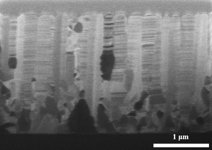
Figure 1 shows the microstructure of the cross-section of a Si/Ag specimen prepared by focused ion beam (FIB). It can be seen that many Ag columnar grains grew normal to the (111)-oriented Si substrate. These Ag grains consisted of a high density of nano-twins piled up on each other. The XRD spectrum of the sputtered Ag film on (111) Si substrate showed a strong Ag (111) peak with very weak Ag (200) and Ag (311) peaks. However, it was found that the sputtered Ag film on (111) Si peeled off easily when the thickness of the Ag film was greater than 2 μm. This result indicated that the adhesion between the nano-twinned film and the (111) Si substrate was insufficient.

To improve the bonding effect of the nano-twinned Ag/(111) Si interface, an adhesive film Ti of 0.1 μm thickness was sputtered on the (111) Si substrate before the deposition of nano-twinned Ag film. In this case, the Ag film on the surface of the Ti-coated (111) Si substrate could be much thicker than the Ag film directly sputtered on Si without the Ti adhesive layer. As shown in Figure 3, the Ag columns grew normal to the (111) Si substrate, similarly to those observed in Figure 1. The columnar Ag grains also contained a high density of nano-twins. The XRD spectrum showed a pure Ag (111) peak, indicating that these nano-twinned Ag film had a very strong (111) preferred orientation.
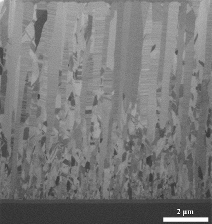
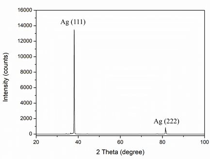
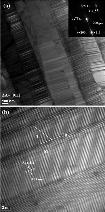
Figure 5 presents a TEM micrograph of the high density of (111)-oriented nano-twinned Ag film. The cross-section SAD pattern shows that the diffraction spots of twin (T) and matrix (M) have a symmetry relationship along the co-plane (1![]() 1)/(
1)/(![]() 1
1![]() ). This revealed that the film was an fcc structure with twin structure. The high-resolution TEM image shows an atomic interplanar spacing of 0.24 nm, indicating that the nano-twinned Ag film was stacked by (111) plane. The twin thicknesses were ranged from 5 to 50 nm, with an average value of about 16 nm.
). This revealed that the film was an fcc structure with twin structure. The high-resolution TEM image shows an atomic interplanar spacing of 0.24 nm, indicating that the nano-twinned Ag film was stacked by (111) plane. The twin thicknesses were ranged from 5 to 50 nm, with an average value of about 16 nm.
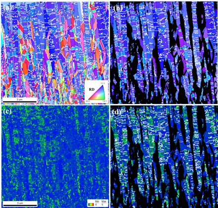
The Ag nano-twins were further identified by electron backscatter diffraction (EBSD) with a scanning step size of 28 nm. It can be seen in Figure 6 that the columnar Ag grains grew primarily along the (111) direction. The average grain size of these Ag columns was 0.17 μm. In Figure 6 (a), the conventional grain boundaries were marked with black lines, the Σ3 coincidence twin boundaries were marked with white lines, and the Σ9 coincidence near-twin boundaries were marked with red lines. The proportions of Σ3 and Σ9 coincidence twin boundaries to the total grain boundaries were 47.2% and 16.2%, respectively. This demonstrated that the (111)-oriented Ag film contained high density twin boundaries. In Figure 6 (b), only the (111) orientation of the nano-twinned Ag film was shown. The proportion of (111)-preferred orientation in the region was calculated to be 63.6%. Figure 6 (c) shows a Kernel Average Misorientation (KAM) figure obtained from EBSD data, indicating the stress distribution of the Ag film. In the KAM figure, green regions possessed relatively higher stress than blue regions, and mostly presented in the (111)-oriented grains, as shown in Figure 6 (d). This stress distribution was caused by high density defects, resulting from high density twin boundaries in (111) columnar grains.
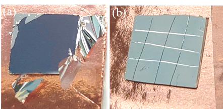
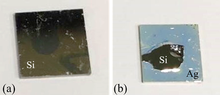
The adhesion of nano-twinned (111) Ag film on the (111) Si substrate with and without a Ti adhesive layer was evaluated using a grid peeling test. Figure 7 (a) shows that, with no Ti adhesive layer, the sputtered Ag film with a thickness of only 2 μm peeled off the (111) Si substrate. With a 0.1 μm Ti adhesive layer inserted between the nano-twinned (111) Ag film and the (111) Si substrate, the Ag film with a thickness of 9 μm exhibited no failure after the peel test, as evidenced in Fig. 7 (b). The results confirm that the addition of a Ti adhesive layer can effectively strengthen the Ag–Si interface and improve the deposition quality of nano-twinned (111) Ag film on (111) Si substrate. In addition, the adhesion strengths were measured by using a thin film pull tester. Figure 8 (a) demonstrates that the nano-twinned Ag film sputtered on Si substrate without the pre-coated Ti was directly separated from the Si substrate, indicating a very poor adhesion strength. In contrast, Ag film sputtered on Ti pre-coated Si substrate possessed an adhesion strength of 17.3 kg/cm2. As shown in Figure 8 (b), it fractured through the Si substrate, and part of Si substrate was pulled up by the stud. This result revealed that the nanotwinned Ag film was more reliable, and can be utilized in engineering applications.
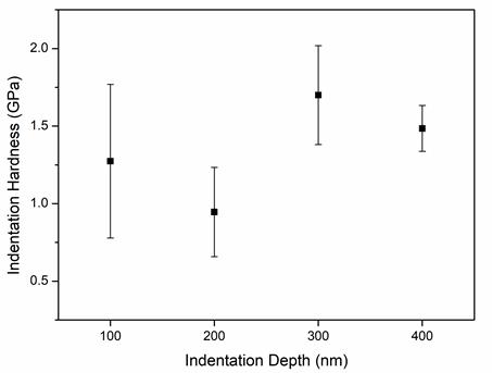
Furthermore, the hardness of nano-twinned Ag film with the thickness of 9 µm was measured by nanoindenter at different indentation depths. Due to the substrate effect and roughness effect, the indentation hardness values are more precise when the depths are greater than 200 nm. Figure 9 shows a maximal hardness value of 1.7 ± 0.3 GPa taken at the indentation depth of 300 nm. It is much larger than the 0.3 GPa of Ag film with normal grains. This result demonstrated that the Ag film possessed an excellent mechanical property, caused by high-density nano-twinned grain structure comprising fine twin thicknesses.
4. Conclusion
Ag films with a high density of nano-twins on (111)-oriented Si substrates have been fabricated by magnetron sputtering. The Ag nano-twins revealed a strong (111) preferred orientation. The Ag grains were observed to grow normal to the (111) Si substrates in a columnar morphology with a diameter of about 0.17 μm. It was also found that directly sputtering the Ag film on the (111) Si substrate caused peeling failure when the thickness of the Ag film was greater than 2 μm. The addition of a Ti adhesive layer with a thickness of 0.1 μm can obviously enhance the bonding effect of sputtering nano-twinned (111) Ag film on (111) Si substrates.
Acknowledgement
This work was supported by the industrial and academic cooperation program of Wire Technology Co. LTD. and the Ministry of Science and Technology, Taiwan, under Grant No. MOST 108-2622-E002-009-CC2 and the Hsinchu Science Park R & D program of Ag Materials Technology Co., LTD. and the Ministry of Science and Technology, Taiwan, under Grant No. 109A18A.
References
[1] T. Watanabe, “An approach to grain boundary design for strong and ductile polycrystals,” Res. Mech., vol. 11, pp. 47-84, 1984.
[2] R.W. Cahn, in Physical Metallurgy, North Holland, 1970, p.1184.
[3] N. Souai, N. Bozzolo, L. Naze, Y. Chastel, R. Loge, “About the possibility of grain boundary engineering via hot-working in a nickel-base superalloy,” Scripta Mater., vol. 62, pp. 851-854, 2010. View Article
[4] S. Mandal, A.K. Bhaduri, V.S. Sarma, “Studies on twinning and grain boundary character distribution during anomalous grain growth in a Ti-modified austenitic stainless steel,” Mater. Sci. Eng. , vol. A 515, pp. 134-140, 2009. View Article
[5] S. Lee, Y.B. Chun, J.W. Hua, S.K. Hwang, “Effect of thermomechanical processing on grain boundary characteristics in twophase brass,” Mater. Sci. Eng., vol. A 363, pp. 307-315, 2003. View Article
[6] C. Pande, B. Rath, M. Imam, “Effect of annealing twins on Hall–Petch relation in polycrystalline materials,” Mater. Sci. Eng., vol. A 367, pp. 171-175, 2004. View Article
[7] L. Lu, Y. Shen, X. Chen, L. Qian, K.Lu, “Ultrahigh strength and high electrical conductivity in copper,” Science, vol. 304, pp. 422-426, 2004. View Article
[8] L. Lu, X. Chen, X. Huang, K.Lu, “Revealing the maximum strength in nanotwinned copper,” Science, vol. 323, pp. 607-610, 2009. View Article
[9] K.C. Chen, W.W. Wu, C.N. Liao, L.J. Chen, K.N. Tu, Science, vol. 321, pp. 1066-1069, 2008. View Article
[10] T.H. Chuang, H.C. Wang, C. H. Tsai, C.C. Chang, C.H. Chuang, J.D. Lee, H.H. Tsai, “Thermal stability of grain structure and material properties in an annealing- twinned Ag-8Au-3Pd alloy wire,” Scripta Mater., vol. 67, pp. 605-608, 2012. View Article
[11] T.C. Liu, C.M. Lin, H.Y. Hsiao, C.L. Lu Y.S. Huang, C. Chen, “Fabrication and characterization of (111)-oriented and nanotwinned Cu by DC electrodeposition,” Crystal growth design, vol. 12, pp. 5012-5016, 2012. View Article
[12] T.C. Liu, H.W. Lin, C.L. Lu, C. Chen, “Effect of grain orientations of Cu seed layers on the growth of (111)-oriented nanotwinned Cu,” Scientific Reports, 4: 6123, DOI: 10.1038/srep06123, 2014. View Article
[13] R. Meyer, L.J. Lewis, “Stacking-fault energies for Ag, Cu, and Ni from empirical tight-binding potentials,” Physical Rev., vol. B 66, p. 052106, 2002. View Article
[14] I.L. Dillamore, R.E. Smallman, W.T. Roberts, “A determination of the stacking-fault energy of some pure FCC metals,” Philo. Mag., vol. 9, pp. 517-526, 1964. View Article
[15] D. Bufford, H. Wang, X. Zhang, “High strength, epitaxial nanotwinned Ag films,” Acta Mater., vol. 59, pp. 93-101, 2011. View Article