International Journal of Mining, Materials, and Metallurgical Engineering (IJMMME)
ISSN: 2562-4571

Volume 8 - Year 2022 - Pages 1-7
DOI: 10.11159.ijmmme.22.001
Solid-Liquid Interdiffusion Bonding between Ti/Ni/Ag/Sn Backside Metallized Si Chips and Cu/Al2O3 - DBC Substrates with Au/Pd/Ni Surface Finish
Kuan-Yu Chiu1, 2 and Pei-Ing Lee1*
1 National Taiwan University, Department of Materials Science and Engineering
No. 1, Sec. 4, Roosevelt Road, Taipei, Taiwan, R.O.C. 10617
JerryChiu@cyntec.com; f07527049@ntu.edu.tw
2 Delta Group Cyntec Company, Ltd.
No. 2, Yanfa 2nd Road, Baoshan Township, Hsinchu County, Hsinchu, Taiwan 308
*Corresponding author: f07527049@ntu.edu.tw
Abstract - In recent years, solid-liquid interdiffusion bonding (SLID) had received much interest from semiconductor manufacturers, primarily due to its ability as a reliable die bonding method especially under high temperatures. This paper presented the work in the optimized Si/Ti/Ni/Ag/Sn bonded on DBC Al2O3/Au/Pd/Ni/Cu substrates by SLID in a vacuum environment. The diffusion phenomenon at the bonding interfaces was observed by SEM/EDX. Well-defined layered bond structures with excellent strength exceeding 7.91 MPa were achieved for the Au-Sn SLID system. Intermetallic compounds in the form of Ag3Sn, Ni3Sn4, and Ni3Sn2 were observed at the bonding interface between Si/Ti/Ni/Ag/Sn wafers and DBC substrates. Superior bond strength of the SLID system allows applications in die bonding that fulfill the requirements of commercial semiconductor packaging specifications.
Keywords: BGBM, SLID bonding, Si/Ti/Ni/Ag/Sn, Intermetallic compound
© Copyright 2022 Authors This is an Open Access article published under the Creative Commons Attribution License terms. Unrestricted use, distribution, and reproduction in any medium are permitted, provided the original work is properly cited.
Date Received: 2021-01-19
Date Accepted: 2021-01-20
Date Published: 2021-02-07
1. Introduction
Backside grinding and backside metallization (BGBM) serves as die attach layer that provide excellent ohmic contact, good heat dissipation, and conductivity to integrated circuits (ICs). The deposition of different metal layers on bare backside silicon is crucial to enhance the thermal conductivity of the wafers. The conventional BGBM wafers consist of a Ti/Ni/Ag structure, in which Ti as the buffer layer to enhance the adhesion between the silicon wafer and the metallization, Ni as the barrier layer to prevent interdiffusion of the metal layers and, Ag as the bonding layer to promote interconnection of die bonding. In some applications, a layer of Sn is deposited on the surface of the backside metallization to prevent the oxidation and sulfidation of Ag. The technology has been a reliable die bonding method for various types of semiconductor devices for high-temperature applications include silicon carbide (SiC), gallium nitride (GaN), gallium arsenide (GaAs) and sapphire semiconductor substrates. Choi et al. has reported the optimized Ag-Sn-Ag thin film structure with outstanding mechanical and electrical performance and evaluated for its application as a replacement for conventional Au-based backside metal [1]. The study has proven that the properties of the Ag/Sn/Ag sandwich structure was superior to that of the conventional Sn/Ag and Ag/Sn structures.
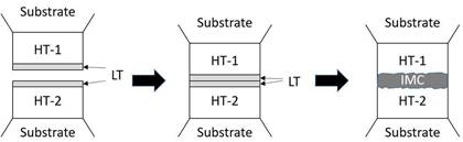
Diffusion welding, also known as solid–liquid diffusion bonding, is a bonding technology based on the principle of isothermal solidification and interface intermetallic compound reaction. Due to the newly formed intermetallic compound has much higher melting point than that of the original low melting point metal thin film intermediate layer, the resulting joint can withstand very high temperatures during operation [2]. According to several literatures, diffusion welding has been widely used in applications such as microwave packages [3], high-power devices [4], thick film resistors [5], GaAs/Si crystal round packages [6], ceramic multi-chip modules [7,8], and even gold jewelry [9]. Recently, diffusion bonding has also been reported in used for MEMS packaging [10,11], semiconductor packaging [9], hybrid connection [12], hermetic packaging [13], and 3D-IC bumps [14]. The technology utilizes a low melting point metal thin film (LT) intermediate layer, which reacts rapidly with the metal layer on a high melting point bulk workpiece or a specific substrate (HT1 and HT2). The original LT intermediate layer is usually thinner than the HT1 and HT2 bulk materials or layers. The solid-liquid interface reaction facilitates the depletion of the LT layer and the conversion between HT1 and HT2 into intermetallic compounds. The diffusion welding process is illustrated in Fig. 2. The combination of both low bonding temperature process and high-temperature applications allows wafer bonding in BGBM processes.
With the rising demand for smartphones, portable devices, computers, USB type-C, e-sports, servers, augmented reality (AR), virtual reality (VR) and automotive electronics, the semiconductor manufacturers are paying more attention on high-power MOSFET electronic components. A power MOSFET is a type of switch designed to handle significant power levels and commonly adapted in power electronics due to its lower power loss and input resistance, ability to withstand large currents, and higher operating frequency. Since power MOSFETs serve as a switch for power devices, the efficient conversion of energy and minimization of loss have become important research directions in the past decades.
A typical silicon foundry process is divided into two main steps: wafer frontside processing and backside processing. The wafer frontside process is where the patterned integrated circuit is made on top of the silicon wafer, known as Front Side Metallization (FSM). The wafer is then undergoing a thinning process to minimize the wafer thickness for high-density packaging so that the on-resistance, RDS(on) can be greatly reduced to fit various advanced packaging. Wafer backside processing begins with backside grinding, etching, surface coarsening and backside metallization. The backside metallization is critical to meet the criteria of electrical, mechanical and thermal requirements of microelectronic devices. Appropriate material selections for the wafer backside metallization often depends on the circuit performance requirements as well as its compatibility with the die attach methods to be employed. Evaporation deposition is commonly used to deposit the desire metal layers on the etched backside wafer due to its strong adhesion metal layers without peeling issues. After a series of CP tests, the wafer is then cut into smaller chips and further joined by a bonding process on another chip or a substrate.
This paper outlines the interdiffusion behavior of Ag, Au and Sn at the bonding interface between Si/Ti/Ni/Ag/Sn and DBC Al2O3 Cu/Ni/Pd/Au as well as the evolution of the growth kinetics of IMCs in a wide temperature range in terms of reliability. Our study focusses on the practical study on real-world applications for electronics assembly. For such purposes, the bonding strength of the samples were measured by a thrust tester. Morphologies and growth kinetics of the IMCs that formed at the bonding interfaces were analyzed before and after aging tests to observe the overall interdiffusion phenomena.
2. Experimental
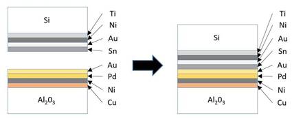
In this study, a pressure of 5 MPa was applied to bonded samples in a vacuum environment at temperatures range from 300 °C to 450 °C for various durations to cause permutation and combination, as illustrated in Fig. 2. After diffusion welding, the samples were then prepared for metallographic grinding and polishing by sand papers with different grit numbers and 1 and 0.3 lm Al2O3 polishing powder after being diced into smaller pieces. The morphology of the bonding interface and the formation of the intermetallic compounds during the welding process were observed by scanning electron microscopy (SEM). Energy dispersive X-ray spectroscopy (EDX) was also used to analyze the chemical compositions of the intermetallic phases. To further evaluate the growth kinetics of intermetallic compounds, the grown thicknesses were measured by SEM images. The bonding strength of the bonded samples were measured by die shear test using a DAGE 4000 bonding tester with a shear speed of 3 × 10⁻⁵ m/s.
3. Result and Discussion
3.1 Reaction Mechanism of Si/Ti/Ni/Ag/Sn Chips with DBC Al2O3 Cu/Ni/Pd/Au Substrates.
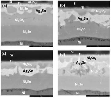
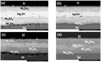
The morphology of the diffusion bonding joints at different bonding conditions were shown in Fig. 3, where IMCs in the forms of Ag3Sn and Ni3Sn2 were detected at the bonding interfaces, indicating the reaction mechanism to be the interdiffusion of solid solutions. As in Fig. 3(a), under bonding temperature of 300oC for 15 minutes, the Sn layer was completely exhausted and reacted with Ag layer to form Ag3Sn. At the same time, some of the Sn diffused towards the Si wafer and reacted with Ni to form Ni3Sn2. Whereby, the remaining Sn diffused to the Ni layer on the DBC substrate to form flame-like IMC Ni3Sn4. The Au (0.1 μm) and Pd layers were so thin that both the thin films depleted throughout the diffusion welding process due to solid-solution effect, so that none of the metals were detected by EDX analysis at the bonding interfaces. Whereas on the DBC substrates, Sn diffused through the DBC metallizations and further reacted with Ni. As the DBC substrates had a much thicker Ni barrier layer (45kÅ) than the Si wafers (3 kÅ), the IMCs formed thereby in the phase of Ni3Sn4.
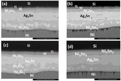
When the bonding duration was increased to 30 min (Fig. 3(b)), the Ag3Sn layer slightly thickened from 0.8 μm to 0.9 μm. The thickness of Ni3Sn2 also slightly increased from 0.2 μm to 0.3 μm, and the amount of Ni3Sn4 formed increased at the DBC substrate side. As the duration was extended to 60 minutes (Fig. 3(c)), the Ni-Sn IMCs were distributed under the Ag3Sn IMC layer, where the IMCs are separated to two distinct Ni3Sn4 and Ni3Sn2. At prolonged heat storage duration of 120 minutes, the Ag3Sn IMC layer had eventually thickened to 1.0 μm.
When the bonding duration was increased to 120 minutes, Sn continued to diffuse towards the Si wafers and developed a thin layer of Ni3Sn4 under the existing Ni3Sn2 layer, as shown in Fig. 3(d). The thickness of the IMC Ag3Sn increased over time by approximately 0.2 µm. No obvious voids or cracks were found at the bonding interface between the Ag3Sn layer in all 4 bonding samples. According to Bud et al., voids often appear at the interface of Ni/Sn/Ni and Cu/Sn/Cu specimens of diffusion welding [15], and such phenomenon was then confirmed by the work by Jacobson et al. [2]. Generally, the Ag/Sn SLID system is a reliable diffusion soldering process with fewer defects at the Ag3Sn interface.
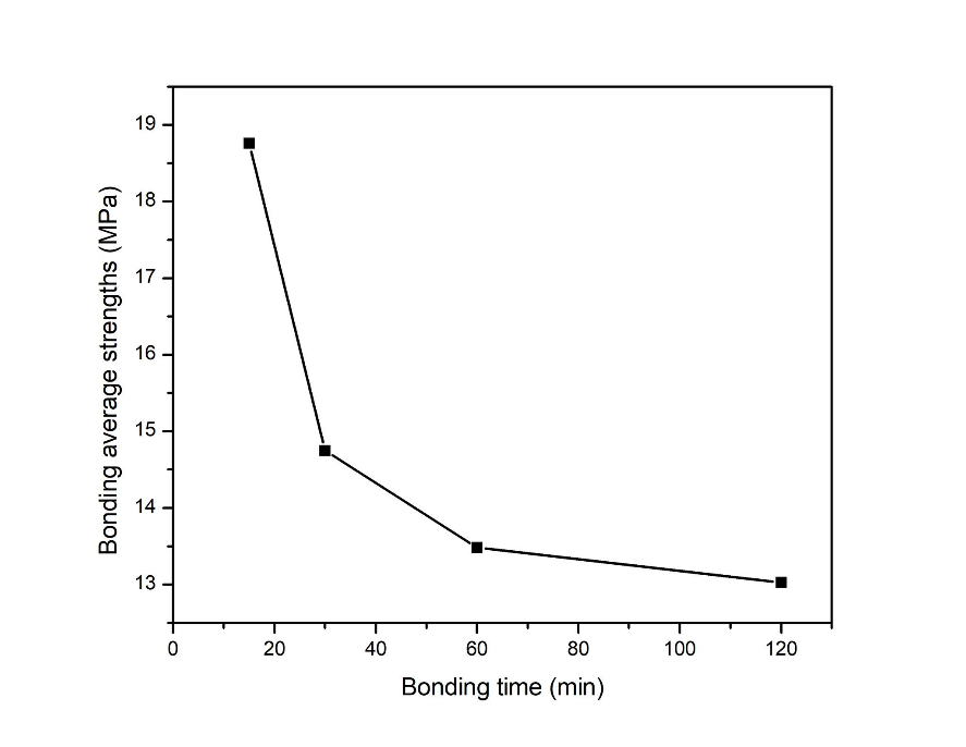
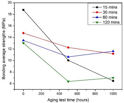
According to the results in Fig. 4, the bonding strengths for diffusion bonding at 300 °C for 15 min to 120 min were plotted in Fig. 4. Across the bonding time, the strength tended to decrease. IMCs with sufficient thickness could contribute much to the bonding strength. With the thin film design of the Si wafers, the intermetallic layers formed was adequate for great bonding interfaces with almost no voids. Within a short period of bonding time required, a good and reliable diffusion bond was formed with an average bond strength of 18.76 MPa. Whereby, it was found that the IMCs Ag3Sn, Ni3Sn4, and Ni3Sn2 formed at the interface showed no direct effect to the bonding strength.
3.2 Aging Test of SLID Bonded Si/Ti/Ag/Sn Chips to DBC Al2O3/Cu/Ni/Pd/Au Substrates
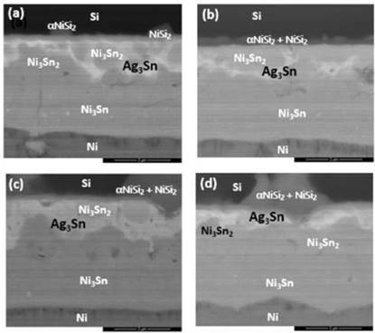
To verify the long-term reliability of the SLID joints, the bonded samples were aged at 400℃ for 500 hours. The average joint strength by thrust tests revealed a decreasing trend with increasing thickness of IMCs formed as illustrated in Fig. 5. The average value was as high as 7.9 MPa, where the lower boundary value was about 4 MPa, and the maximum average achieved 45.42 MPa by the bonded samples at 450oC for 30 minutes, which all the samples had met the requirements of commercial semiconductor packaging specifications. The intermetallic compounds Ag3Sn, Ni3Sn4, and Ni3Sn2 were observed. Interestingly, the failure position of the shear test was found to be at both the interface of the Si wafer and within the IMCs. Previous study had reported that the fracture strength of (100)-oriented silicon wafers has fracture toughness of 0.95 MPa, 0.90 MPa for silicon (110) wafers, and 0.82 MPa for silicon (111) wafers [14]. The IMCs formed at the bonding interfaces had also contributed to the bonding strength and support to the thinner BGBM wafers. The morphologies of the aged joints were examined by SEM and EDX analysis as in Fig. 6. As compared to the unaged samples, the IMC layers grew enormously due to the interdiffusion of Ni and Sn and vigorous reactions between the two metals. The thickened IMC layers were believed to contribute to the reduction of joint strength. In addition, a portion of Ni was found at the Si/Ti interface and reacted with Si to form αNiSi2 IMC. The aging of the joints for long period injected large amount of heat into the metal layers, causing Ni atoms to excite and diffused through the Ti barrier layer. Such phenomenon could degrade the integrity of the Si/Ti interface and increase the risk of short circuit of the overall device.
Meanwhile, the average thrust values of each sample group after aging at 400oC for 1000 hours differed little from those after aging test for 500 hours under the same temperature. This proved that after high temperature and longer-term aging, the bonded structures were still remained rigid without much degradation in tensile strength. In other words, the die bonded structures had achieved high reliability even after exposure to extreme conditions. Fig. 7 showed the morphology of the IMCs at the bonding interface of the bonded couples after aged at 400oC for 1000 hours, where the amount of IMCs at the interface continued grew thicker. Localized voids formed with the increased thickness of the overall bonding layer, which was highly related to the diffusion rates of the elements. Similar phenomenon was observed in prolonged aging time in which Ni diffused through the Ti barrier layer to the Si/Ti interface and generated larger area of αNiSi2 intermetallic compound.
3.3 Enhanced SLID Bonding Temperature of Si/Ti/Ni/Ag/Sn Chip Bonded with DBC Al2O3/Cu/Ni/Pd/Au Substrates
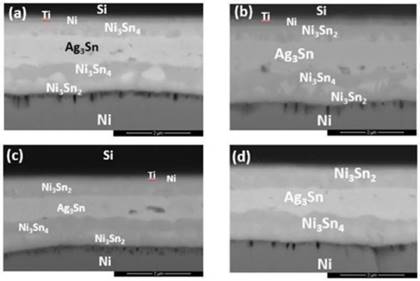
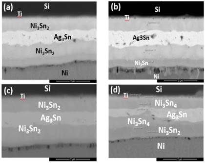
However, further increasing the diffusion welding temperatures to 350°C, 400 °C and 450°C, the thin Ni3Sn4 and Ni3Sn2 layers started to transform into thicker Ni3Sn4 and Ni3Sn2 layers, as in Fig. 8-10. Small local cracks were observed at the interface of the Ni layer and Ag3Sn and at that of DBC and Ni3Sn2, which caused the bonding strength to degrade. As the increased bonding temperatures had induced the accelerated diffusion rate of the elements, where Ni atoms diffused through the Ti barrier layer and reached the Si/Ti interface. At the Si/Ti interface, Ni reacted with Si to form αNiSi2 intermetallic compounds. Therefore, bonding at lower temperatures and shorter bonding period can prevent the undesired diffusion of Ni layer.
4. Conclusion
Solid–liquid diffusion bonding is an effective bonding method to join backside metallized Si wafers to DBC substrates. Sn interlayer diffusion bonding was applied at temperatures of 300oC - 450°C for periods of 15 - 120 minutes to join the Si/Ti/Ni/Ag/Sn chips with DBC Al2O3/Cu/Ni/Pd/Au. The Sn interlayer reacted with the Ag and Ni layers to form an Ag3Sn and Ni3Sn2 intermetallic compounds. Au and Pd layers depleted during the bonding process due to solid-solution effect. The Ni3Sn4 intermetallic phase also formed between the Ag3Sn IMC and the Cu electrode. After aging at 400°C, the Ni atoms diffused through the Ti barrier layer and reacted with Si to form αNiSi2 intermetallic compound. The formation of intermetallic compounds had separated the wafer from the metallization layers and degraded the thermal and electrical conductivities of the overall structure. According to the thrust tests, it was found that the Ag-Sn SLID systems had shown satisfactory bonding strengths and met the requirements of commercial electronic packaging specifications. Average bonding strength as high as 18.76 MPa was achieved with such low bonding temperature at 300oC for short period of 15 minutes allowed further applications in the semiconductor industries to replace the conventional Au backside metals. With appropriate materials and metallization structure designs, the solid–liquid diffusion bonding method provides great potential to the development of BGBM technology and wide applications in various electronic products.
Acknowledgements
This study was sponsored by the Hsinchu Science Park R&D program of Ag Materials Technology Co., Ltd. and the Ministry of Science and Technology, Taiwan, under Grant No. 109A18A.
References
[1] J. S. Choi and S. J. An, “Backside Metallization of Ag-Sn-Ag Multilayer Thin Films and Die Attach for Semiconductor Applications”, Journal of Electronics Materials, vol. 49, no. 7, pp. 4265-4271, 2020. View Article
[2] D. M. Jacobson and G. Humpston, “Diffusion Soldering”, Soldering & Surface Mount Technology, vol. 10, pp. 27-32, 1992. View Article
[3] D. M. Jacobson and S. P. S. Sangha, “A Novel Lightweight Microwave Packaging Technology”, IEEE Transactions on Components, Packaging, and Manufacturing Technology A, vol. 3, pp. 515-520, 1998. View Article
[4] D. M. Jacobson and S. P. S. Sangha, “Novel Application of Diffusion Soldering”, Soldering & Surface Mount Technology, vol. 8, pp. 12-15, 1996. View Article
[5] P. K. Khanna, S. K. Bhatnagar, G. Dalke, D. Brunner, and W. Gust, “Development of Thermally Stable Ni-Ag Interconnections for Application to Resistive Films”,Mat. Sci. Eng. B, 33, pp. 6-9, 1995. View Article
[6] Y. C. Chen, W. W. So, and C. C. Lee, “A Fluxless Bonding Technology Using Indium-Silver Multilayer Composites”, IEEE Transactions on Components, Hybrids, and Manufacturing Technology, vol. 20, pp. 46-57, 1997. View Article
[7] T. H. Chuang, H. J. Lin, and C. W. Tsao, “Intermetallic Compounds Formed During Diffusion Soldering of Au/Cu/Al2O3 and Cu/Ti/Si with Sn/In Interlayer”,Journal of Electronics Materials, vol. 35, pp. 1566-1570, 2006. View Article
[8] M. W. Liang, T. E. Hsieh, S. Y. Chang, and T. H. Chuang, “Thin-Film Reactions during Diffusion Soldering of Cu/Ti/Si and Au/Cu/Al2O3 with Sn Interlayers”,Journal of Electronics Materials, vol. 12, pp. 452-455, 2003. View Article
[9] D. M. Jacobson, G. Humpston, and S. P. S. Sangha, “Diffusion Soldering a New Low Temperature Process for Joining Carat Gold Jewelry”, Gold Bulletin, vol. 26, pp. 90-104, 1991. View Article
[10] W. C. Welch, III, J. Chae, and K. Najafi, “Transfer of Metals MEMS Packages using a Wafer-Level Solder Transfer Technique”, IEEE Transactions on Advanced Packaging, vol. 28, pp. 643-649, 2005. View Article
[11] R. I. Made, C. L. Gan, L. L. Yan, A. B. Yu, S. W. Yoon, J. H. Lau, and C. Lee, “Study of Low-Temperature Thermocompression Bonding in Ag-In Solder for Packaging Applications”, Journal of Electronics Materials, vol. 38, pp. 365–371, 2009. View Article
[12] G. A. Lo´pez, S. Sommadossi, P. Zieba, W. Gust, and E. J. Mittemeijer, “Kinetic Behaviour of Diffusion-Soldered Ni/Al/Ni Interconnections”, Mater. Chem. Phys., vol. 78, pp. 459–463, 2002. View Article
[13] F. Bartels, J. W. Morris Jr., G. Dalke, and W. Gust, “Intermetallic Phase Formation in Thin Solid–liquid Diffusion Couples”, Journal of Electronics Materials, vol. 23, pp. 787-790, 1994. View Article
[14] W. R. Runyan, “Silicon Semiconductor Technology”, McGraw-Hill, U.S.A, pp. 223-229, 1965.
[15] S. Bader, W. Gust, and H. Hieber, “Rapid Formation of Intermetallic Compounds Interdiffusion in the Cu-Sn and Ni-Sn Systems”, Acta Metall. Mater., vol. 43, pp. 329-337, 1995. View Article
[16] T. H. Chuang, W. T. Yeh, C. H. Chuang, and J. D. Hwang, “Improvement of bonding strength of a (Pb, Sn)Te-Cu contact manufactured in a low-temperature SLID bonding process”, Journal of Alloys and Compounds, vol. 613, pp. 46-54, 2014. View Article
[17] Y. C. Lin, C. L. Yang, J. Y. Huang, C. C. Jain, J. D. Hwang, H. S. Chu, S. C. Chen and T. H. Chuang, “Low-Temperature Bonding of Bi0.5Sb1.5Te3 Thermoelectric Material with Cu Electrodes using a Thin-Film In Interlayer”, Metallurgical and Materials Transactions A, vol. 47, no. 9, p. 4767-4776, 2016. View Article
[18] C. L. Yang, H. J. Lai, J. D. Hwang and T. H. Chuang, “Diffusion Soldering of Bi0.5Sb1.5Te3 Thermoelectric Material with Cu Electrode”, Journal of Materials Engineering and Performance, vol. 22, no. 7, p. 2029-2037, 2013. View Article