Volume 8 - Year 2022 - Pages 08-15
DOI: 10.11159.ijmmme.22.002
Mechanism of the Evaporation of Ag Nano-Twinned Films on Si Wafers with Assistance of Ion Beam Bombardment
Tung-Han Chuang*1, 2, Yin-Hsuan Chen1*, Po-Ching Wu1,3
1 Institute of Materials Science and Engineering, National Taiwan University, 106 Taipei, Taiwan.
2 Ag Materials Technology Co., AMTC, Hsinchu Science Park, 30078 Hsinchu, Taiwan.
3 Taiwan Semiconductor Manufacturing Co., TSMC, Hsinchu Science Park, 30078 Hsinchu, Taiwan.
*Corresponding author: tunghan@ntu.edu.tw
tunghan@ntu.edu.tw; sammichen8815@gmail.com; brian19960510@gmail.com
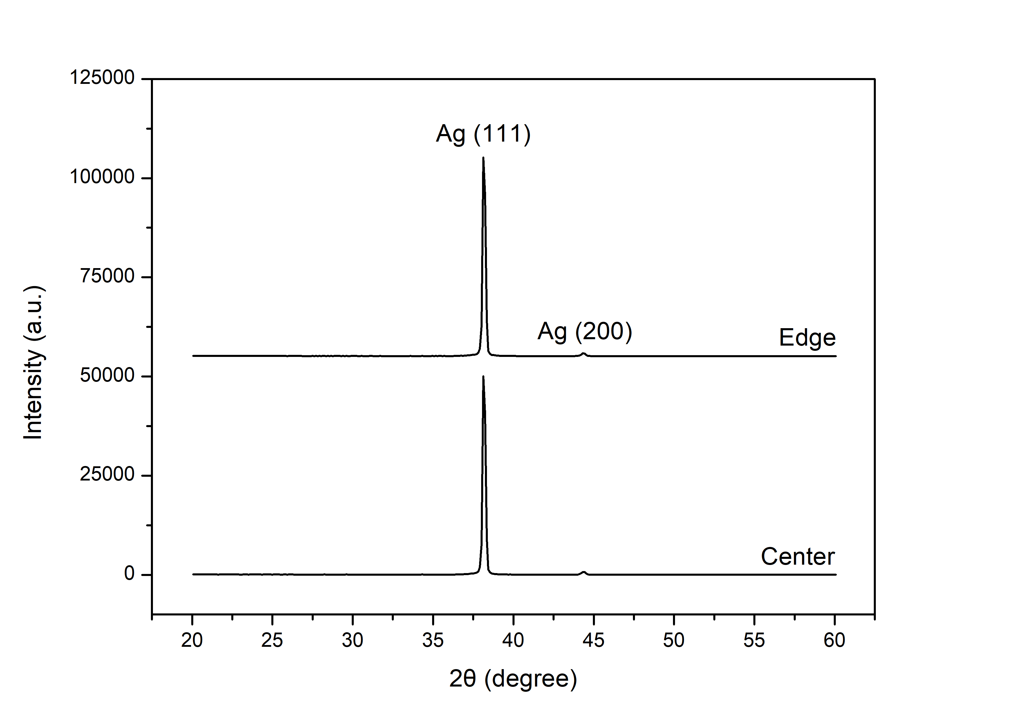
Abstract - Ag nanotwinned thin film with a thickness of about 4 μm has been evaporated on an 8-inch Si wafer with the assistance of ion beam bombardment. FIB cross-sectional imaging revealed many columnar grains with an average width of about 0.5 μm containing numerous parallel Ag nanotwins. The XRD spectrum showed a strong Ag (111) peak without any other crystal orientations both in the central and edge regions, indicating the (111) preferred orientation of the Ag nanotwinned films. The results were consistent with top-view EBSD inverse pole figure analysis showing a very high density of the (111) orientation, 85.2±1.9%, on the surface of the Si wafer. A modified stress relaxation model is proposed to explain the enhancement of the formation of a high density of nanotwins in the Ag films evaporated with simultaneous ion bombardment.
Keywords: Ag nanotwin; deposition, ion bombardment, (111) preferred orientation, stress relaxation
© Copyright 2022 Authors This is an Open Access article published under the Creative Commons Attribution License terms. Unrestricted use, distribution, and reproduction in any medium are permitted, provided the original work is properly cited.
Date Received: 2022-12-02
Date Accepted: 2022-12-12
Date Published: 2022-12-22
1. Introduction
For the manufacturing of power modules, backside grinding and backside metallization (BGBM) are the most important processes in forming a good ohmic contact and an optimum surface for further die bonding with direct bonding copper (DBC) substrates. Backside metallization must meet the electrical, mechanical and thermal requirements of power modules. The selection of the materials for backside metallization depends on the circuit performance as well as its compatibility with the die bonding methods to be employed, and conventional Ti/Ni/Ag multi-layer thin films have been used [1]. In this typical backside metallization structure, the Ti acts as an adhesive layer on Si the wafer, and the Ni functions as a barrier layer to prevent the exhaustion of the Ti adhesive thin film due to interfacial reactions during the die bonding process. In addition, coarse-grained Ag thin films are commonly chosen as the reaction layer on the top surface of backside metallization multi-layered thin films.
For the die bonding of power IC chips with DBC ceramic substrates, traditional soldering and Ag sintering methods are commonly employed. However, a soldered module cannot endure high temperatures during operation. In contrast, the Ag sintering method has the disadvantage of high porosity, poor conductivity and material damage. An alternate method of direct bonding that is believed to be more reliable than traditional soldering at high operation temperature is to employ Ag sintering for less porosity and lower electrical resistivity [2]. Using the principle of solid-state reaction, certain innovative direct bonding methods can be performed at very low temperature, even below the bonding temperature of soldering [3]. Recently, a low temperature direct bonding technique employing high density (111) textured nanotwinned films has attracted much attention for its potential for application in 3D-IC advanced packaging and die bonding in high power modules [4, 5].
It is known that the contact and non-contact regions at the interface of direct bonding metals result in creep deformation through the surface diffusion of atoms from the strained region to the unstrained region (void) under thermal compression, leading to new atomic bonds across the interfaces. Juang et al. has demonstrated a Cu-to-Cu direct bonding technique that uses an electroplating (111) oriented Cu nanotwinned (nt-Cu) thin film [6]. An alternative approach for Cu-to-Cu direct bonding through Cu nanotwinned films was reported by Liu et al. That approach exhibited excellent bonding quality with virtually no voids at the smooth bonding interface after bonding at a temperature lower than 150 ℃ for a short time of 30 minutes [7]. Upon further investigations into the characteristics of other nanotwinned films employed in low temperature direct bonding, Au nanotwins with a high density of (111) orientation have been fabricated with a periodically-reversed electroplating process by Wu et al. [8]. With control of the surface roughness, the Au-to-Au direct bond demonstrated a satisfactory performance wherein all of the bonded samples failed at either the film/substrate layer or the Si substrate, implying a stronger bonding strength than the maximum shear strength of 40.8 MPa determined with bond-testing equipment. In FCC metals, as twin boundaries form in their preferred states to release strain, the stress-relaxed nanotwinned film can be of lower energy than the strained structure. Similar to that of Cu, the diffusion rate of the (111) surface is much higher than that of other surfaces in Au, driving atoms to diffuse along the surface and increasing the likelihood of successful direct bonding.
Chuang et al. further showed that Ag nanotwinned films with a highly (111) orientation can provide certain benefits as compared with electroplated Cu nanotwinned film, such as higher atomic diffusivity and electrical conductivity, better oxidation resistance and lower direct bonding temperature [9]. They sputtered nanotwinned Ag films on Si chips with (100), (110) and (111) orientations pre-coated with Ti thin films and reported that the resulting Ag films had a high density of (111) textured nanotwins with twin spacing of 2 to 50 nm. The cross-sectional FIB micrographs showed that the thickness of the transition layers with conventional random grains that formed at the bottom of Ag films deposited on various orientations of Si chips had a sequence of Si (100) < Si (111) < Si (110) [10].
Among the many deposition processes, such as evaporation, electroplating, or chemical vapor deposition (CVD), sputtering has the advantages of good thin film adhesion, sound process stability and quality control. The method is also capable of depositing a wide variety of metals, insulators, alloys and composites. By reversing the applied voltage on the electrodes, in-situ cleaning prior to film deposition can be performed to remove oxides or contaminants on the substrates. On the other hand, the evaporation method has the benefits of a high deposition rate and low substrate damage during the deposition process. In addition, evaporated film has excellent purity due to the high vacuum condition. Most importantly, the process is relatively cheap as compared with other deposition techniques and is therefore the one most popularly applied for the backside metallization of power IC wafers in industry [11].
The mechanism of forming nanotwin structures has recently become a research topic of great importance. Numerous theories have been introduced to explain the occurrence of twinning [12, 13]. Although the cause of twinning formation has been discussed from various viewpoints, its fundamental origin can be simply addressed via energy analysis. A crystal structure with a continuous lattice exhibits the lowest free energy state of that collection of atoms. Thus, variation from such a structure could result in an increase in the energy of the bound atoms. The formation of twins creates a lattice distinct from the matrix. The twin boundary is established at the region where twin and matrix meet to fulfil the minimum interfacial energy requirement. The twin boundary is a single plane of atoms connecting two non-mixing phases. Such an arrangement ensures that the structural change across the twin boundary is less abrupt, as there is no significant lattice discontinuity. Therefore, whilst the energy level at a twin boundary is higher than that in the rest of the crystal, the difference in energy levels is negligible. Similar phenomena of close-minimum energy can also be observed within all types of intergrowths, where the crystal orientation across the intergrowth boundaries behaves akin to the crystal orientation across twin boundaries.
For the formation of high density (111) oriented textured Cu nanotwinned films by pulse electroplating, Xu et al. proposed a stress relaxation model wherein the stress generated by island coalescence during the electroplating process is relieved by recrystallization and grain growth [14]. Using first principles calculations of the total crystal binding energy, they showed stress relaxation to be the driving force for nanotwin formation. Therefore, it was suggested that, during pulse electrodeposition of Cu films, highly-strained recrystallized grains of Cu grew to relieve stress and formed strain-relaxed nanotwins. Through in-situ stress measurements during the pulse electroplating of nanotwinned Cu films, Xu et al. further observed an abrupt increase in tensile stress to about 400 MPa in the pulse-on stage and a stress relaxation in the pulse-off stage [15]. They also predicted that complete relaxation of the tensile stress allowed the formation of Cu nanotwins with twin spacing of about 28 nm, which was quite consistent with the TEM observations. Chan et al. reported that a dense nanotwinned structure could be induced by high-energy (5 keV) Ar+ ion bombardment on an electroplated Cu film at low temperature (from 25 °C to -175 °C). The mechanism of formation of such Cu nanotwins was ascribed to the high-energy ion bombardment causing thermal spike cascades and generating twinning partial dislocations [16]. However, the energy of the ion bombardment was much lower than that used by Chan et al. during the evaporating process, and the mechanism of nanotwin formation seemed not to be correlated to the thermal spike cascades. For the evaporation of uniform nanotwinned films on Si wafers, a modified stress relaxation model was proposed. Furthermore, Yu et al. suggested that the removal of stacking-fault tetrahedra by twin boundaries may result in the formation of nanotwins [17].
2. Experimental Study
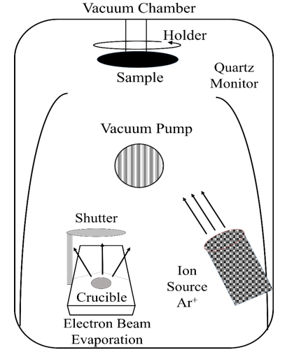
In this study, a high-density (111) oriented Ag nanotwinned film was first deposited on 8-inch Si wafers by evaporation. To increase the adhesion of the Ag thin films with the Si wafers, an additional Ti thin film with a thickness of 0.1 µm was pre-coated on the Si substrates. Then the Ag films were deposited by electron beam evaporation on the nanotwinned film deposited Si wafer with an ion beam-assisted deposition system as shown in Fig. 1. The base pressure was lower than 5 × 10⁻⁶ Torr (6 × 10⁻⁴ Pa) and the working pressure was set at 1.5 × 10⁻⁴ Torr (2 × 10⁻² Pa) with Ar of 16.7 sccm as the ion source. The ion beam voltage and current were set at 240 V and 5 A, respectively. The deposition rate of Ag was 1.8 nm/s.
After the evaporation process, the specimens were cut from the central and edge regions of the Ag nanotwinned film deposited Si wafer. For the observations of the cross-sectional grain structures, a focused ion beam (FIB, Hitachi NX2000) was employed. The grain boundary orientations of the nanotwins were analyzed by electron backscatter diffraction (EBSD, JEOL JSM-7800F). In addition, the overall crystal orientations and texture of the Ag nanotwinned films were identified by X-ray diffraction (XRD, Rigaku TTRAX). Transmission electron microscopy (TEM, FEI Tecnai G2 F20) was used for the microstructure analysis of the Ag nanotwins.
3. Results and Discussions
A typical FIB microstructure of the cross-section of a conventional backside metallized Ti/Ni/Ag multi-film evaporated on an 8-inch Si wafer without ion beam bombardment is shown in Fig. 2. In the figure, equiaxial coarse Ag grains with an average grain size over 300 nm can be observed on the Ti/Ni coated Si substrate. In addition, the Ag outer layer did not react with the Ni barrier layer, resulting in spalling at the Ni/Ag interface. Since the Ni thin film in the Ti/Ni/Ag backside metallization acted as a barrier layer for a further die bonding process using soldering or Ag sintering, it can be omitted in the direct bonding method. Juang et al. also reported that the atomic diffusivity of the (111) orientation surface is 3 to 5 orders of magnitude higher than those of (110) and (100) surfaces, leading to a decrease in the Cu-to-Cu bonding temperature to 150.
The problem of Si/Ti interfacial precipitation reaction cannot occur at such a low temperature. Therefore, an innovative backside metallization structure of Ag nanotwinned film deposited by evaporation on a Ti pre-coated Si wafer without a Ni barrier layer was evaluated in this study.
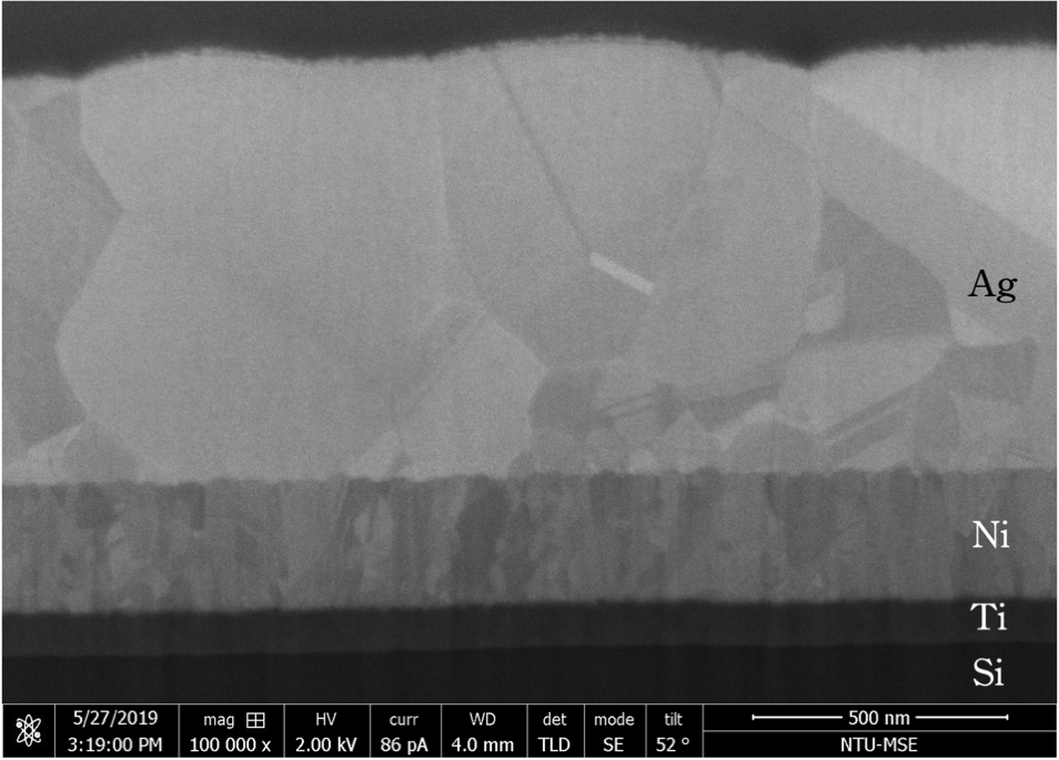
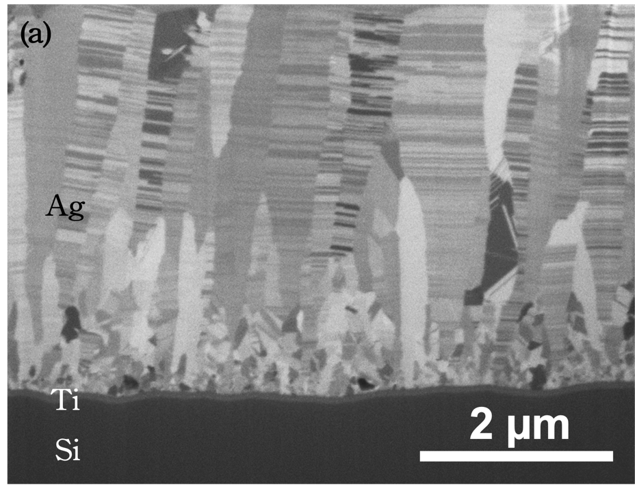
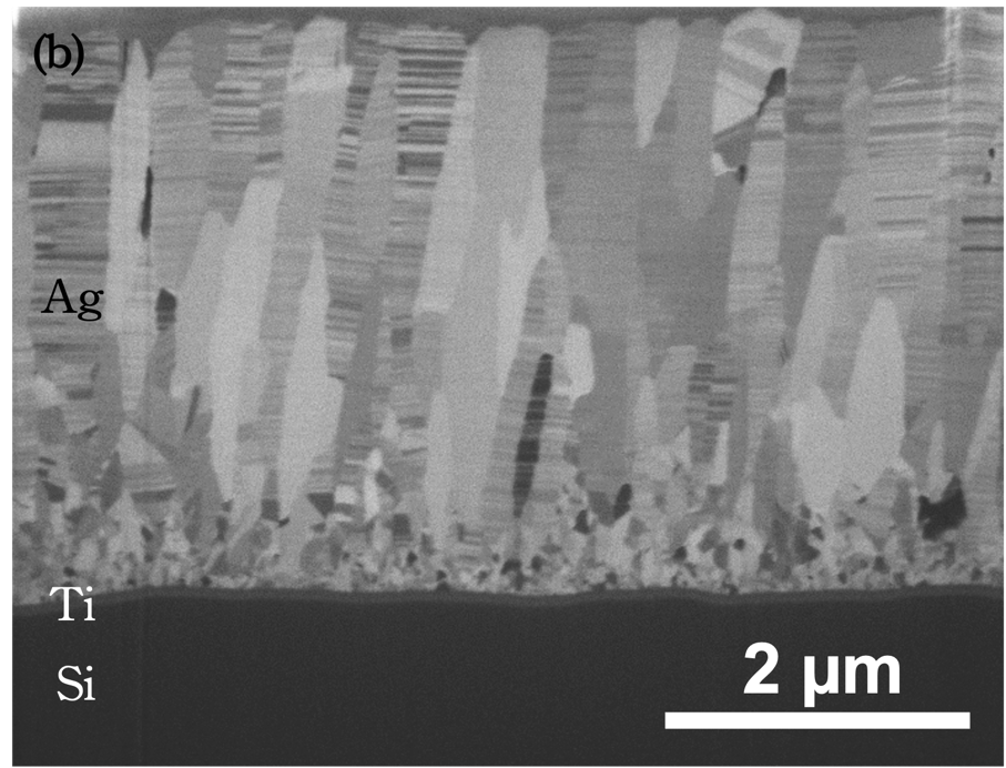
Figure 3 shows that evaporation of an Ag thin film with a thickness of about 4 μm on a Ti pre-coated 8-inch Si wafer assisted with ion beam bombardment resulted in a very different grain structure. In this case, columnar grains comprising a high density of densely-packed nanotwins appeared in the central region of the deposited Ag film, as evidenced in Fig. 3a. A similar Ag nanotwinned structure can also be observed in the edge region of the evaporated Si wafer shown in Fig. 3b. The columnar grains had an average width of about 0.5 μm and contained numerous parallel Ag nanotwins. It is worthwhile to mention that the transition layers below the Ag nanotwinned either in both the central and edge regions of the 8-inch Si wafer were thinner than 1 μm. The results indicated that the Ag nanotwinned film evaporated on this 8-inch Si wafer was excellent in both quality and uniformity. Furthermore, the XRD spectrum shown in Fig. 4 indicated that the Ag nanotwinned films sputtered on Si wafers had a strong Ag (111) peak comparing to other crystal orientations, in both the central and edge regions, confirming the highly (111) textured characteristics of the Ag nanotwins.
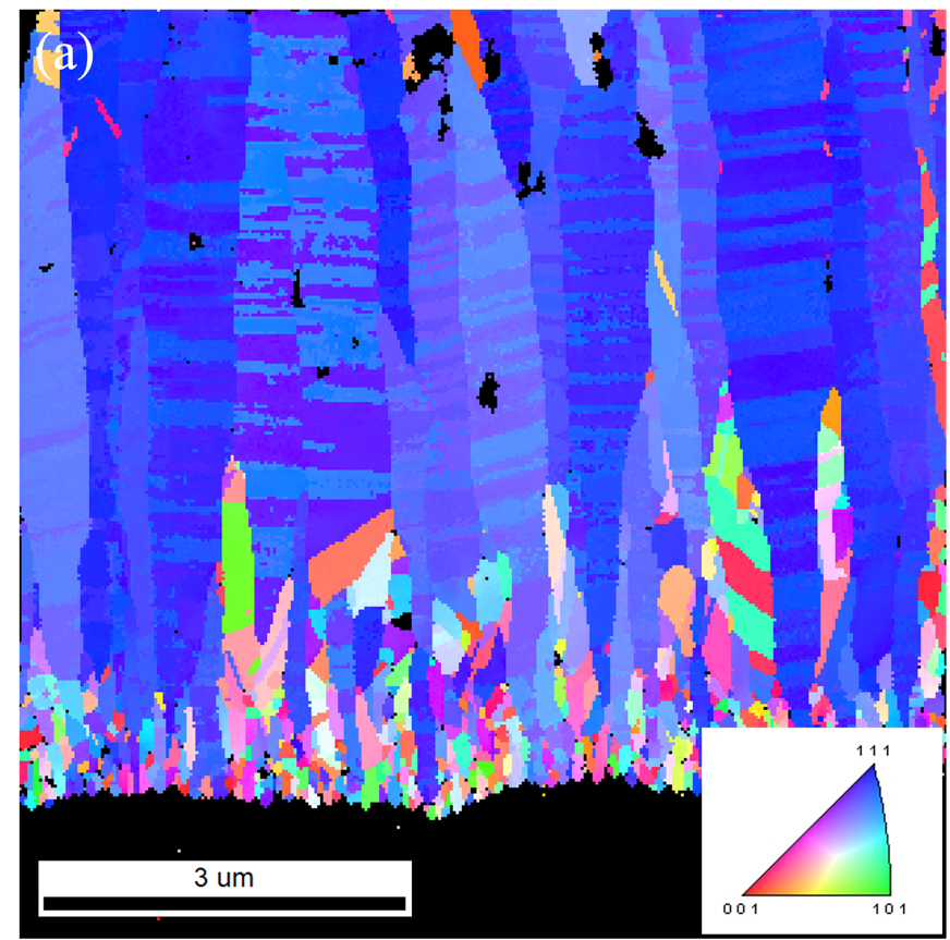
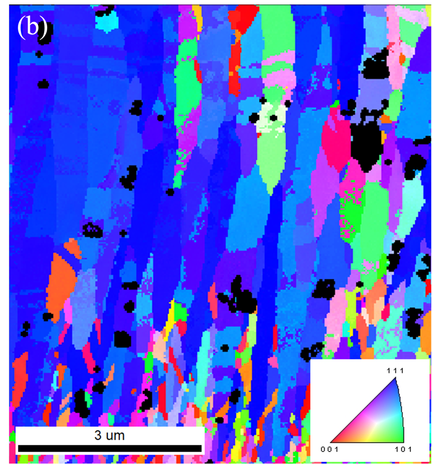
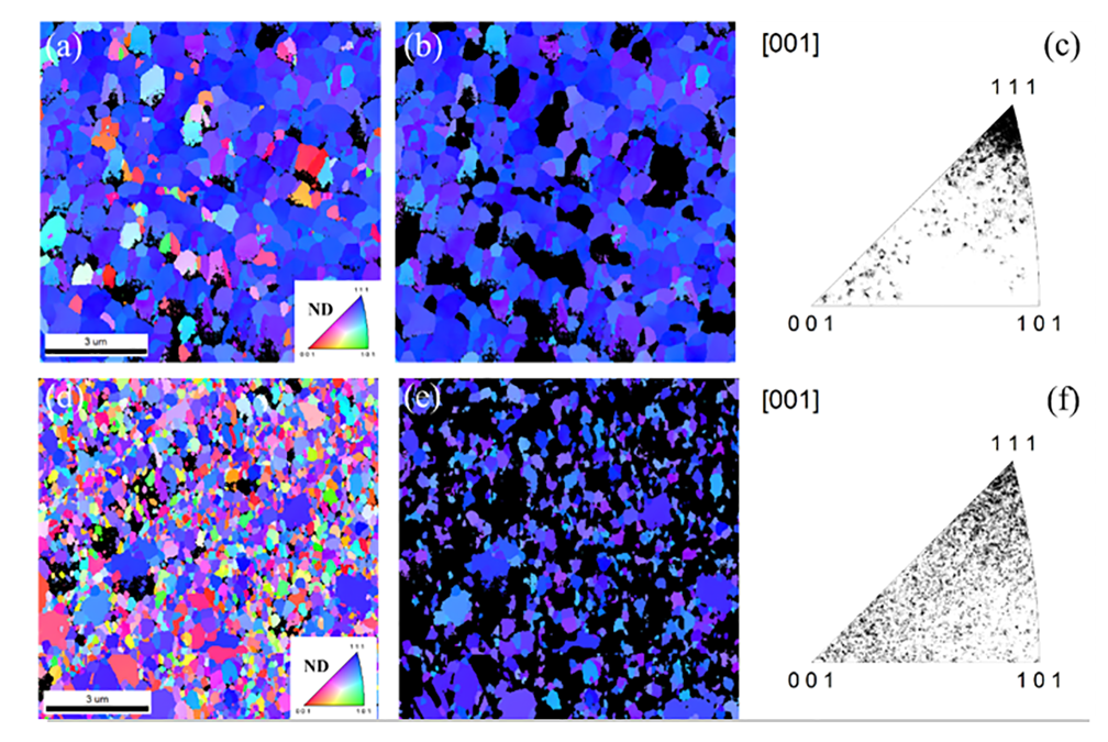
The distribution of the crystal orientations in the boundaries in Ag nano-twinned films sputtered on Si wafer was identified by electron backscatter diffraction (EBSD). The cross-sectional EBSD image in Fig. 5 shows that the columnar grains grew normal to the Si wafer and primarily along the <111> direction. The proportions of coincident Σ3 twin boundaries to the total grain boundaries in the Ag films in the central and edge regions of the Si wafer reached 49.9±2.7% and 37.7±2.3 %, respectively. It was obvious that the Ag film had a very high twin density, confirming the FIB cross-sectional metallography in Fig. 2. The top-view EBSD inverse pole figure mapping revealed in Fig. 6a to 6c further shows a very high density of the (111) orientation, 85.2±1.9%, on the surface of the Si wafer. In contrast, in the Ag nanotwinned film evaporated without ion beam bombardment, a low density of the (111) orientation, 42.8±2.1%, was obtained on the top surface, as shown in Fig. 6d to 6f. It was also found that the proportion of coincident Σ3 twin boundaries of the Ag nanotwins evaporated on this Si wafer without ion bombardment was only 19.6±2.5%, as determined from the cross-sectional EBSD image; this was about half of the nanotwin density achieved with ion beam bombardment.
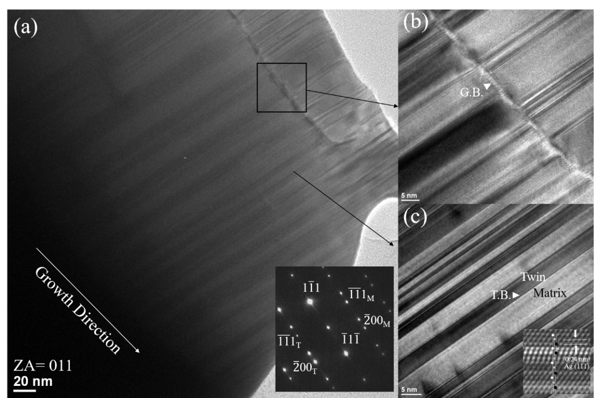
The typical microstructure and the crystal orientation of the evaporated Ag nanotwins on Si wafer was identified from the TEM image in Fig. 7a. The twin characteristics of the grain structure in the Ag thin film were evidenced by the symmetry relationship between the (¯("1" ) ¯("1" ) "1" )M/(¯("2" ) "00" )M and (¯("1" ) ¯("1" ) "1" )T/(¯("2" ) "00" )T diffraction patterns from the inset selected area electron diffraction (SAED) analysis in Fig. 7a taken along the [011] zone axis. The M and T marks labelled on the patterns represent the diffraction dots of the matrix and twins, respectively, and the 3 diffraction dots in the middle represent the co-plane (1¯("1" )1)/(¯("1" )1¯("1" )) of the matrix and twins. Figure 7b shows a high-resolution TEM image of the parallel nanotwins in the Ag thin film evaporated on Si wafer. In Fig. 7b, it can also be seen that an amorphous interface existed at the intersection of the boundaries of neighbouring column grains in the Ag nanotwinned film. The twin spacing, measured from the HR-TEM micrographs in Fig. 7b and 7c, ranged from 2 to 15 nm, with an average value of about 6 nm. Finally, it can be observed in Fig. 7c that the Ag (111) twin boundaries revealed a very fine atomic spacing of about 0.24 nm.
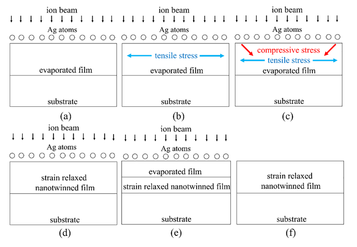
For clarification of the enhancement effect of ion beam bombardment during the evaporation process, a modified stress relaxation model based on the mechanism of Xu et al. [13, 14] is schematically presented in Fig. 8. It is suggested that, during the solidification of the Ag liquid film deposited on Si wafer, the large difference between the thermal expansion coefficients (CTE) of Ag (19.1 x 10⁻⁶ K-1) and Si (4.7-7.6 x 10⁻⁶ K-1) induces large tensile stress in the deposited Ag film (Fig. 8a and b). Simultaneously, ion beam collisions introduce compressive stress in the solidified Ag film, similarly to the shot peening phenomenon (Fig. 8c). The compressive stress from the ion beam bombardment relieves the tensile stress (Fig. 8d), resulting in the formation of strain-relaxed nanotwins (Fig. 8e). Further evaporation of the liquid Ag film and subsequent solidification, accompanied by the tensile and compressive stress relaxation from the ion beam assistance, leads to the growth of nanotwinned Ag film (Fig. 8f).
4. Conclusion
Ag nanotwinned thin film with a highly (111) crystal orientation has been deposited on an 8-inch Si wafer using the evaporation method assisted with ion beam bombardment. The spacing of nanotwin boundaries as measured from the HR-TEM image ranged from 2 to 15 nm with an average value of about 6 nm. Cross-sectional EBSD images indicated that the proportions of coincident Σ3 twin boundaries to the total grain boundaries in the Ag films in the central and edge regions of Si wafer reached 49.9±2.7% and 37.7±2.3%, respectively. Top-view EBSD inverse pole figure mapping showed a very high density of the (111) orientation, 85.2±1.9%, in contrast to the low value of 42.8±2.1% in the Ag nanotwinned film evaporated without ion beam bombardment. To explain the mechanism underlying the enhanced nanotwin formation in Ag films deposited with simultaneous ion bombardment, a modified stress relaxation model is proposed; it is suggested that the tensile stress in solidified deposited Ag film is relieved by the compressive stress introduced by the ion bombardment, resulting in the formation of strain relaxed nanotwins.
Acknowledgements
This study was sponsored by the Hsinchu Science Park R&D program of Ag Materials Technology Co., LTD. and the Ministry of Science and Technology, Taiwan, under Grant No. 109A18A.
References
[1] M. Ciacchi, H. Eder, and H. Hirscher, Evaporation vs. Sputtering of metal layers on the Backside of Silicon wafers, 2006. IEEE/SEMI Advanced Semiconductor Manufacturing Conference, pp. 99-103.
[2] S. H. Christiansen, R. Singh and U. Gosele. Wafer Direct Bonding: From Advanced Substrate Engineering to Future Applications in Micro/Nanoelectronics. Proceedings of the IEEE. 94 (2006), pp. 2060-2106. View Article
[3] C.T. Ko and K.N. Chen. Low temperature bonding technology for 3D integration. Microelectronics reliability 52-2 (2012), pp.302-311. View Article
[4] Z. Y. Zheng, Y. T. Huang, Z. Y. Wang, M. Y. Zhang, W. T. Wang, C. C. Chung, S. J. Cherng, Y. H. Tsai, P. C. Li, Z. G. Lu, C. M. Chen and S. P. Feng. Electrodeposition of (111) oriented and nanotwin-doped nanocrystalline Cu with ultrahigh strength for 3D IC application. Nanotechnology. 32 (2021), pp. 225702-225712. View Article
[5] T.H. Chuang, P.C. Wu, Y.C. Lai, and P.I. Lee, "Low Temperature Direct Bonding of 3D-IC Packages and Power IC Modules using Ag Nanotwinned Thin Films", Int. J. Mining, Mater. and Metall. Eng., accepted (2022). View Article
[6] J.Y. Juang, C.L. Lu, K.J. Chen, C.C.A. Chen, P.N. Hsu, C. Chen and K.N. Tu. Copper-to-copper direct bonding on highly (111) oriented nanotwinned copper in no-vacuum ambient. Scientific reports, 8(1), (2018), pp.1-11. View Article
[7] C. M. Liu, H.W. Lin, Y.C. Chu, C. Chen, D. R. Lyu, K. N. Chen and K.N. Tu. Low-temperature direct copper-to-copper bonding enabled by creep on highly (1 1 1)-oriented Cu surfaces. Scripta Materialia, 78 (2014), pp.65-68. View Article
[8] J.A. Wu, C.Y. Huang, W.W. Wu and C. Chen. Fabrication of (111) oriented Nanotwinned Au Films for Au-to-Au Direct Bonding. Materials 11(11), (2018), pp.2287. View Article
[9] Y.C. Lai, P.C. Wu, and T.H. Chuang, 2021, "Characterization of Interfacial Structure for Low Temperature Direct Bonding of Si Substrates Sputtered with Ag Nanotwinned Films", Mater. Character., 175 (2021) 111060, 1-12. View Article
[10] T.H. Chuang*, P.C. Wu, and Y.C. Lin. "Lattice buffer effect of Ti film on the epitaxial growth of Ag nanotwins on Si substrates with various orientations." Materials Characterization, 167, 110509, 2020. View Article
[11] P.C. Wu, T.H. Chuang*. "Evaporation of Ag nanotwinned films on Si substrates with ion beam assistance." IEEE Transactions on Components, Packaging and Manufacturing Technology, accepted, 2021.
[12] G. Sun, X. Q. He and J. Lu. Nanotwinned and. Hierarchical Nanotwinned Metals: A Review of Experimental, Computational and. Theroetical Efforts. Npj Computational Materials. 4 (2018), pp. 1-18. View Article
[13] L. Sun, X. He & J. Lu. Nanotwinned and. Hierarchical nanotwinned metals: a review of experimental, computational and. theoretical efforts. NPJ Computational Materials 4, (2018), pp.1-18 View Article
[14] D. Xu, W.L. Kwan, K. Chen, X. Zhang, V. Ozoliņš, K.-N. Tu, Nanotwin formation in copper thin films by stress/strain relaxation in pulse electrodeposition, Applied Physics Letters 91(25) (2007) 254105. View Article
[15] D. Xu, V. Sriram, V. Ozolins, J.-M. Yang, K.-N. Tu, G.R. Stafford, C. Beauchamp, In situ measurements of stress evolution for nanotwin formation during pulse electrodeposition of copper, Journal of Applied Physics 105(2) (2009) 023521. View Article
[16] T.-C. Chan, Y.-Z. Chen, Y.-L. Chueh, C.-N. Liao, Large-scale nanotwins in Cu films/Cu nanowires via stress engineering by a high-energy ion beam bombardment process: growth and. Characterization Journal of Materials Chemistry C 2(46) (2014) 9805-9812. View Article
[17] K. Y. Yu, D. Bufford, C. Sun, Y. Liu, H. Wang, M. A. Kirk, M. Li and X. Zhang. Removal of stacking-fault tetrahedra by twin boundaries in nanotwinned metals. Nature Communications. 4 (2013), pp. 1-7. View Article

