International Journal of Mining, Materials, and Metallurgical Engineering (IJMMME)
ISSN: 2562-4571

Volume 9 - Year 2023 - Pages 1-8
DOI: 10.11159.ijmmme.2023.001
Characterization of High Density (111)-oriented Ag Nanotwinned Films Deposited on Sapphire Wafers
Yin-Hsuan Chen1, and Tung-Han Chuang*1,2
1Institute of Materials Science and Engineering, National Taiwan University, 106 Taipei, Taiwan.
Address, City, Country
2Ag Materials Technology Co., LTD, Hsinchu Science Park, 30078 Hsinchu, Taiwan.
sammichen8815@gmail.com; tunghan@ntu.edu.tw
*Corresponding author: tunghan@ntu.edu.tw
Abstract - The exceptional properties of nanotwinned structures have been a hot area of research in recent years. Silver (Ag) has the lowest stacking fault energy (SFE) among all FCC metals, which has a strong tendency to form a twin structure. Also, sapphire substrates are ideal for use in LED applications due to high-temperature resistance, high strength, good electrical insulations, and low dielectric loss. Depositing Ag nanotwinned films on sapphire substrates can serve as a perfect candidate for die bonding in LED manufacturing. In this study, both sputtering and evaporating methods had been demonstrated for the fabrication of high density (111)-textured Ag nanotwinned films on sapphire wafers. Microstructural analyses show that both the sputtered and evaporated Ag grains presented a high density of twin structure. The cross-sectional EBSD analysis of the sputtered Ag nanotwinned film indicated a highly (111)-preferred orientation to 34.6% of the overall grains. Further, the sputtering process allows the production of surface roughness of the Ag nanotwinned film up to 65.1 nm. The epitaxial growth of Ag nanotwinned films with (111)-preferred orientation can be utilized by both the deposition methods
Keywords: Nanotwins, sputtering, evaporation, (111)-preferred orientation, sapphire substrates.
© Copyright 2023 Authors This is an Open Access article published under the Creative Commons Attribution License terms. Unrestricted use, distribution, and reproduction in any medium are permitted, provided the original work is properly cited.
Date Received: 2023-06-26
Date Revised: 2023-08-10
Date Accepted: 2023-08-21
Date Published: 2023-09-11
1. Introduction
In recent years, LEDs (light emitting diodes) have received great attention due to the advantages of high brightness, long lifetime, and most importantly, low energy consumption [1]. Large amount of energy losses in an incandescent light bulb in the form of heat energy when electrical energy is converted to light energy. Therefore, it is critical to design a LED lighting system capable of efficient heat dissipation to ensure long-term reliability. In fact, substrates have a direct relation with the optical performance of LEDs especially in the heat dissipation. Therefore, appropriate selection of the substrate materials for LED modules should feature fine-matched lattice parameters and thermal expansion coefficient, chemically stable, and good physical and mechanical properties [2]
Sapphire, also known as α-aluminum oxide, α-Al2O3, has a hexagonal lattice unit cell with lattice parameters of a = b = 4.758 Å, c = 12.992 Å;at room temperature [3]. As is known to all, the material has benefits such as high hardness and mechanical strength, excellent chemical and thermal stability due to its high ionic inter-atomics bonds. Moreover, other unique material properties, including excellent wear and corrosion resistance, substantial thermal and electrical conductivity, low cost, and exceptional optical transparency make sapphire ideal for a variety of applications. Today, sapphire wafers are being extensively used for epitaxial growth of III-V and II-VI based LEDs, such as gallium nitride (GaN). These LEDs are fabricated by the epitaxial growth of nitride semiconductor layers on sapphire substrate by various growth techniques available [4-6].
According to the Hall-Petch relation, the grain size determines the properties of the materials. Smaller grain size increases the tensile strength and tends to increase the ductility of the materials. As grain size refinement up to nanoscale occurs, it is normally expected that with grain boundaries now occupying a significant volume fraction of the material, and thus plays a critical role in the deformation of the materials. In contrast to high angle boundaries, twin boundaries can improve mechanical strength without compromising the high ductility of the materials. Consequently, nanoscale twinning in polycrystalline materials usually embed with enhanced mechanical strength and electrical conductivity in comparison with the bulk structure. [7] The coincident site lattice (CSL) boundaries are boundaries with misorientations that exhibit a high fraction of lattice sites in coincidence compared to normal grain boundaries. A low Σ signifies high coincidence, which has been reported variety of macroscopic properties improvement as the density of low Σ CSL boundaries increases. Twin boundary is the simplest form of coincidence boundaries, which has a reciprocal density of common lattice points of 3, also known as Σ3. [8]. Previous research in molecular dynamics (MD) simulations has proven that the twin boundaries act as strong barriers to dislocation transmission as it requires high shear or tensile stress to move the dislocations across the twin interfaces. In this case, both Σ3(111) coherent twin boundary (CTB) and Σ3(112) incoherent twin boundary (ITB) serve as obstacles for dislocation transmission to occur [9-11]. This is largely because the formation of Σ3 coincidence site lattice can lower the interfacial energy by up to 5% comparing to the interfacial energy of normal grain boundaries [12]. With lower interfacial energy, various outstanding mechanical properties are reported, including higher strength, hardness, ductility, enhanced diffusivity, and thermal stability [13], superior magnetic properties in comparison with conventional polycrystalline materials.
Silver has been well known as a representative FCC metal with a low stacking fault energy of about 22 mJ/m2 when compared to other metals with FCC structures. It is known that lower stacking fault energy promotes the formation of twin structures [14]. In other words, low SFE metals tend to exhibit significantly higher dislocation densities and as consequence, higher formation of twin structure. Moreover, Ag also presents better electrical and thermal conductivity combine with high-temperature stability, which shows huge potential for application. Till date, the metal has been widely used in GaN LED structure as the reflection layer to promote light extraction efficiency [15].
The fabrication of thin films with preferred orientation is traditionally processed by electroplating and magnetron sputtering. In the past, copper (Cu) film with preferred orientation has been intensively studied. According to Chen et al., electroplating with high current and high stirring speed allows successful fabrication of nanotwinned Cu with film thickness up to 20 µm [16]. Sun et al. have also demonstrated the growth mechanism of preferentially oriented columnar Cu film with nanotwinned structure on silicon wafer by direct-current electrodeposition process with acid addition [17]. Nanotwinned Cu films formed in acidic Cu sulfate electrolyte with [18,19] and without additives [20] by electrodeposition has also been studied. However, electroplating could cause severe environmental issues, leading to sputtering and evaporating deposition as alternatives, which are relatively environmental-friendly. Thin film deposited by sputtering is well bonded onto the substrate, with high purity, excellent film quality, and good uniformity on a large-area substrate. At the same time, the repeatability of the magnetron sputtering process is good, which allows the process to become industrialized. The island coalescence mechanism, which was originally proposed by Hoffman, explained a reasonable growth mechanism for thin films. When there is an attractive interatomic force between adjacent islands, the film is strained. The elastic displacement of the film leads to the coalescence of the islands and finally forms a continuous film. Therefore, the residual stress state of the sputtered films could simply cause high-density twin formation as twins will form to accommodate to relieve residual strains [21]. By applying negative substrate bias during deposition, positively charged Ar ions will be attracted to the substrate and induce ion bombardment, which generates compressive stresses toward the film. With proper parameters, the formation of nanotwinned structure can be achieved. Many other research have reported preferred-oriented Al [22], Ag [23], Pd [24], Cu [25], and 330 stainless steel [26] thin film produced by magnetron sputtering.
Electron beam evaporation, however, is a physical vapor deposition process with low substrate temperature and high deposition rate, as well as a more economical operation for thin film fabrication. Therefore, it has been widely used to deposit various kinds of metals and alloys especially in the semiconductor industries to integrate electronic devices with metal contacts. Unfortunately, few reports about the evaporation deposition of a high-density nanotwinned film with preferential crystal orientation have been done. Although Wang et al. [28] and Idrissi et al. [24] synthesized a Pd nanotwinned structure on Si substrates by electron beam evaporation, they found that the films exhibited random orientation, and the twin densities are much lower than those of nanotwinned films manufactured by sputtering or electroplating methods. At the same time, Chuang et al. has also reported evaporation of Ag nanotwinned films on Si substrates with ion beam assistance [30].
In this study, both sputtering and evaporating processes are applied to fabricate high density (111)-oriented Ag nanotwinned film on (001)-sapphire substrates. We also evaluate the influence of difference deposition methods to the Ag nanotwinned structure. The resulting microstructures with different deposition methods are investigated and analysed in the following discussions, which could have direct effects on the application of Ag in the LEDs manufacturing.
2. Experimental
Both magnetron sputtering and evaporation deposition are applied to deposit the highly <111>-oriented Ag films with thickness of 4 µm onto (001)-sapphire substrates. Half portion of the specimens are precoated with Ti as the adhesive layers for a thickness of 100 nm. For the magnetron sputtering process, the chamber was evacuated to vacuum of 5×10⁻⁶ torr and the working pressure of 5×10⁻³ torr before deposition starts. For film thickness of 4 µm, the deposition rate of Ag films is 0.85 nm/s with a sputtering power of 150W. Whereby for the electron beam evaporation process, an ion beam-assisted system is applied to induce ion bombardment to the deposited films. The base pressure is set below 5×10⁻⁶ torr and the working pressure is at 1.5×10⁻⁴ torr with 4.5 sccm of argon (Ar) gas flow as ion source. The ion beam voltage and current are 60 V and 0.4 A, respectively.
After deposition, the specimens are examined with various characterizations. X-ray diffraction (XRD) is used to determine the crystal orientation of the surface of Ag film. The cross-sections of the microstructures are observed by a focused ion beam (FIB). Electron backscatter diffraction (EBSD) analysis is performed to analyze the density of preferred crystal orientation. Transmission electron microscopy (TEM, FEI TTRAX) is employed to further study the microstructure of the cross-sections. Selected area electron diffraction (SAED) patterns obtained from the TEM cross-sections to reveal the atomic structure of the Ag thin films.
3. Results and Discussion
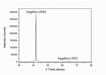
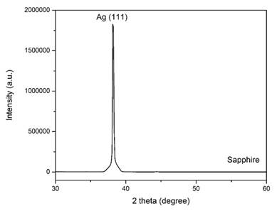
The XRD spectrum of sapphire wafer is measured in the 2θ= 30-80 degree range by using a X-ray diffraction meter with a Cu Kα radiation source (λ= 0.154 nm). As shown in Figure 1, it is clearly observed that the wafer shows a strong sapphire (001) peak at about 41.6o with a small peak (205) at about 64.5o. The existence of the strong (0001) diffraction peak confirms a high crystallinity of the sapphire substrate. Reported by numerous research, epitaxy growth on c-cut sapphire has known by far the most optimal option due to its better crystallinity [31], and strong photoluminescence emission [32,33].
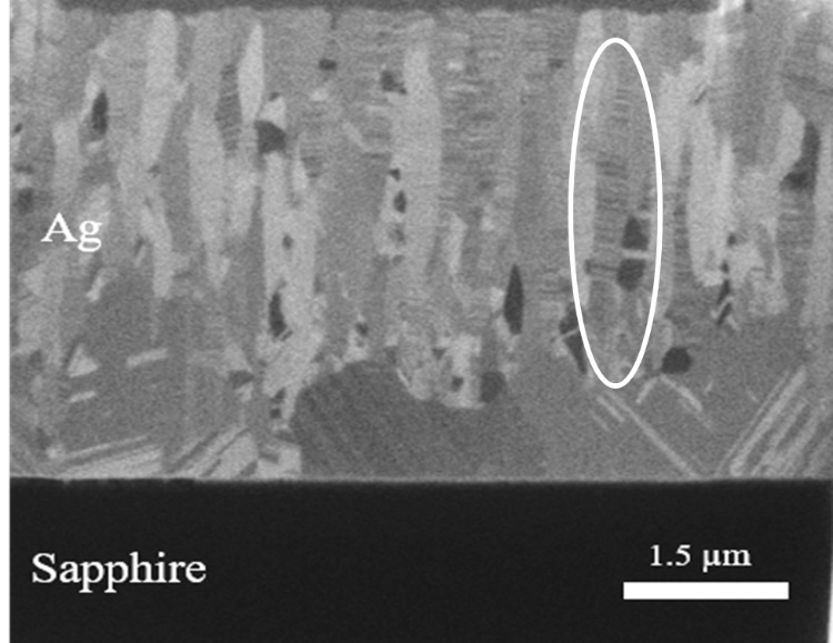
The cross-sectional micrograph of Ag film sputtered directly on the sapphire substrate without any adhesive layer exhibit small amount of columnar structure as circled in Figure 2.
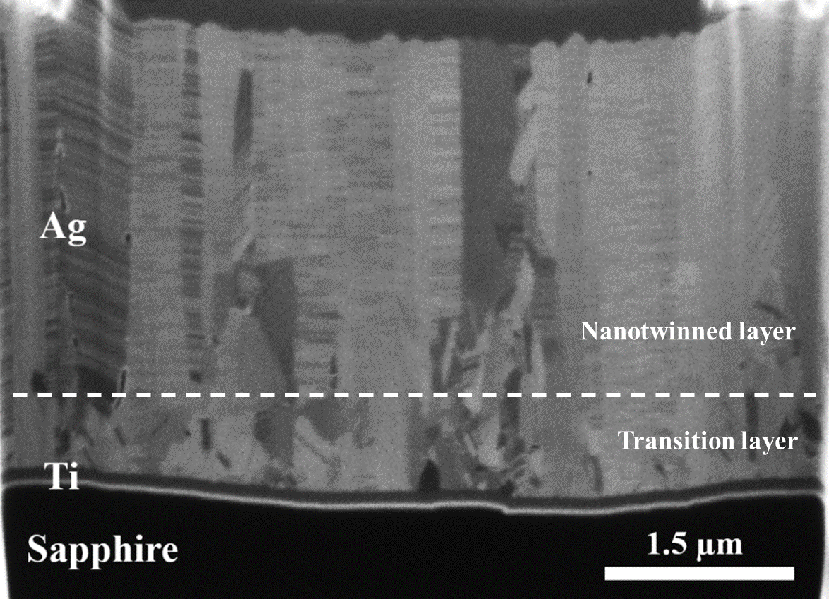
The thickness of the transition layer was determined by measuring the distance from the boundary of Ag/Ti or Ag/Sapphire to the top of the deposited Ag nanotwinned thin film at 10 equally-spaced points on the FIB micrograph and calculating the average thickness.
These columnar grains in figure 2 consist of high density of nanotwins piling up on each other in a twin spacing of few nanometers. Also, the equiaxial coarse annealing twin layer with a thickness of 1.425±0.19 µm appear below the Ag columnar structure, which are believed to form by the effect of heat during the deposition process. Due to its low stacking fault energy, Ag readily forms twins during the deposition process. However, the formation of coarse annealing twins indicates a thicker transition layer and reduction of Ag columnar nanotwins formed within the Ag thin film. In fact, the equiaxed grains are relatively poor in thermal stability and therefore thicker transition layer is prone to abnormal grain growth at elevated temperatures.
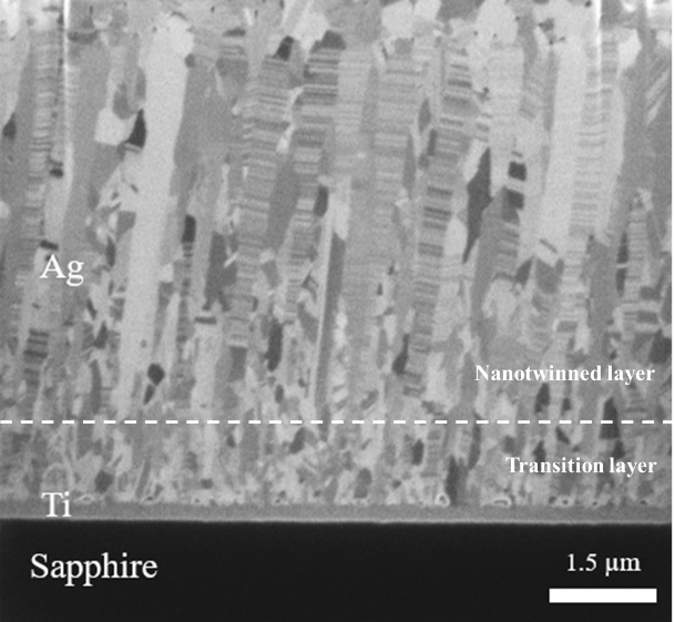
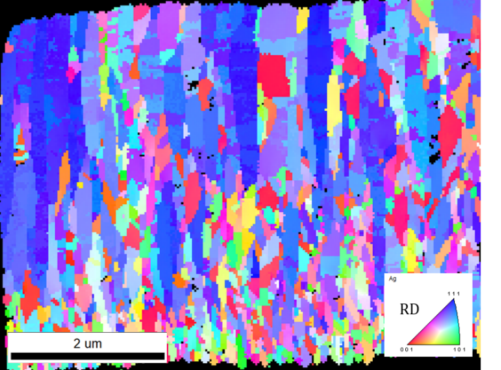
To mitigate the lattice mismatch between Ag and sapphire wafer, a Ti adhesive layer is usually added between the sapphire substrate and Ag film for better bondability. Figure 3 shows the cross-sectional FIB image micrograph of nanotwinned Ag films sputtered on sapphire substrate with a layer of Ti adhesive layer. As known to all, Ti shares the property of adhering well onto substrate materials. In addition, thin layer of Ti (probably 0.1 μm) does not typically alter the property of the device that is fabricated. The sites in the thin adhesion layer serve to promote nucleation of the Ag thin film which might not properly adhere on the substrate, resulting the film to flake off from the substrate. Apparently, higher density of Ag nanotwins is observed within columnar grain structure with finer equiaxial grains in a thinner transition layer (1.166±0.19 µm), indicated by the dashed line. The transition layer is usually being treated as defects as these fine equiaxed grains are prone to abnormal grain growth during subsequent wafer bonding process. Therefore, a thinner transition layer is often more desirable for better thermal stability of the overall. The high-resolution EBSD orientation map for the cross-sectional Ag film is shown in Figure 4. Grains marked blue are oriented with the (111) plane parallel to the substrate surface, consisted of 34.6% of the overall microstructure. The fine equiaxial grains in different colors are of random orientations. The orientation of fine equiaxial grains is mostly random. Again, the XRD spectrum in Figure 5 founds a strong intensity of Ag (111) peak without any other impurities peaks and is consistent to the EBSD analysis.
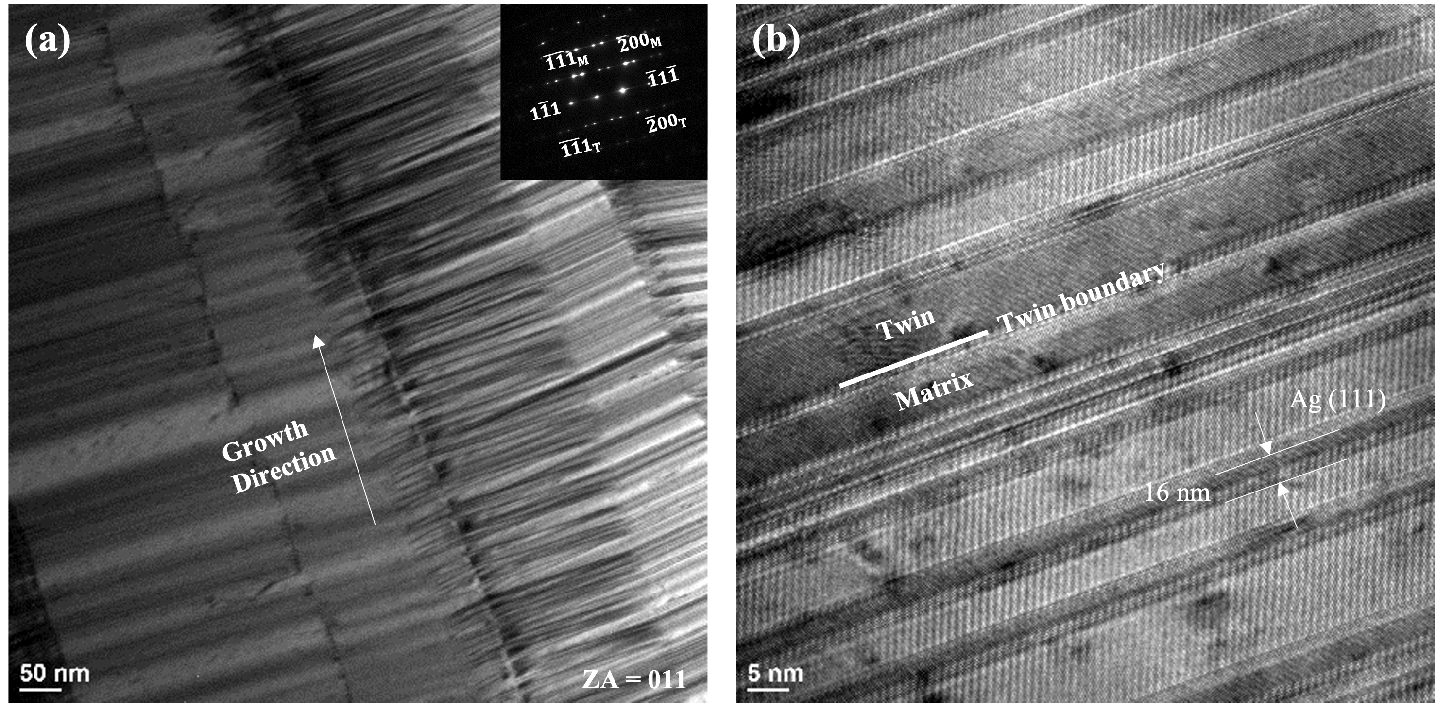
In addition to FIB imaging, the nanotwinned structure of the sputtered Ag nanotwin structure is further investigated by transmission electron microscopy (TEM) film. Figure 6 (a) shows the cross-sectional bright-field TEM images of the Ag film sputtered on Ti pre-coated sapphire substrate, taken along the zone axis of [011]. High density of stacking nanotwins are observed along the columnar grains, whereby the twin interfaces are parallel to the substrate surface. In the SAD pattern, the matrix and twin diffraction spots showed spot splitting across the {111} twin interfaces, which are identified to be stacking faults. Statistical measurement of the twin spacing indicated an average of 16 nm, as evident from the HR-TEM image in Figure 6 (b). The fast Fourier transform of the film has confirmed a typical (111)-oriented twin structure, which is consistent with the XRD analysis in Figure 5.
On the other hand, the cross-sectional FIB micrograph of the evaporated Ag film on sapphire substrate is shown in Fig. 7. Similar to the sputtered Ag film, the evaporated Ag film consists of numerous Ag columnar structure with high density of nanotwins stacking on each other. Since formation of columnar nanotwinned structure can be relatively difficult for evaporated Ag films, an additional ion bombardment is applied to the deposited film during evaporation [30]. The effect of ion bombardment during evaporation deposition seems to be accounted for the formation of high density (111)-oriented Ag nanotwins on sapphire substrate. However, the equiaxed grains within the transition layer are larger than that of the sputtered film. The result should be regard as the effect of high energy by ion bombardment during deposition process and cause a significant grain growth of the equiaxed grains [35]. The relationship between surface energy and strain energy provides a reasonable explanation for the phenomenon [36]. According to the structure zone model, the low energy ion bombardment remains at zone T of the film structure, in which the film texture changes to wider columns with preferred orientation parallel to the densely populated plane, in this case (111)-orientation. This is due to the further promotion of thermally enhanced surface diffusion owing to an increase of substrate temperature resulted by the ion bombardment. Therefore, columnar structure with highly (111)-preferred orientation is expected with proper control of deposition parameter.
Furthermore, the surface topography of the nanotwinned Ag film sputtered on the (001)-oriented sapphire pre-coated with Ti film was analysed by the Atomic Force Microscopy (AFM). The 3D-AFM plot in Figure 8 revealed unevenly distributed hillocks on the surface of the sputtered Ag film. The surface roughness of the nanotwinned Ag film sputtered on this sapphire substrate reached a much larger value of 65.1 nm in comparison to those of GaAs [37] and SiC [38] substrates as listed in Table 1. However, the cross-sectional FIB images indicated that no extra-large columnar grain was found on the surface of the nanotwinned Ag thin film. The appearance of such an uneven AFM image might be attributed to the rough surface morphology of the as received sapphire substrate. The results evidenced that the surface roughness of deposited Ag nanotwinned films for various substrates did reveal an apparent substrate-related effect. It is suggested that an adequate surface grinding and polishing for the as received sapphire wafers is necessary.
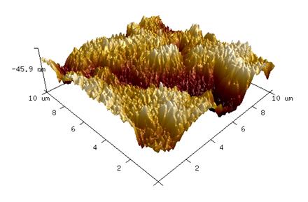
Table 1. Surface roughness of sputtered nanotwinned Ag film on various substrates with thickness of 4 µm.
|
Type of Substrates |
Surface roughness (nm) |
|
GaAs |
5.6 |
|
SiC |
13.4 |
|
Sapphire |
65.1 |
4. Conclusion
In this study, we demonstrate synthesis of highly (111)-oriented Ag nanotwinned thin film can be synthesized by both sputtering and evaporation deposition methods. For both deposition processes, the FIB micrographs show a high density of nanotwinned structure in the Ag columnar grains. EBSD analysis report about 34.6 % of the grains are of (111)-orientation in Ag nanotwinned film fabricated by the sputtering process. The XRD result also confirm the strong intensity of (111) orientation of sputtered Ag film. The introduction of high density nanotwins in Ag thin film on sapphire substrates by both sputtering and electron-beam evaporation is believed to play an important role in low-temperature interconnections in wafer level bonding, which has valuable properties for applications in the LED industries.
5. Acknowledgements
This study was sponsored by the Hsinchu Science Park R & D program of Ag Materials Technology Co., LTD. and the Ministry of Science and Technology, Taiwan, under Grant No. 109A18A.
References
[1] Tang, Huili, Hongjun Li, and Jun Xu. "Growth and development of sapphire crystal for LED applications." Advanced Topics on Crystal Growth (2013): 307-333. View Article
[2] Pandher, Ranjit, Pandher, R., Bhatkal, R., Lang, K.J., & Semiconductors, O. O. "Impact of Substrate Materials On Reliability of High Power LED Assemblies." (2016): 25-29.
[3] Cao, Linlin, Cao, L., Zhang, X., Yuan, J., Guo, L., Hong, T., Hang, W., & Ma, Y. "Study on the influence of sapphire crystal orientation on its chemical mechanical polishing." Applied Sciences 10.22 (2020): 8065. View Article
[4] Ebnesajjad, Sina, and Cyrus Ebnesajjad. Surface treatment of materials for adhesive bonding. William Andrew, 2013. View Article
[5] Huang, Jian-Jang, Hao-Chung Kuo, and Shyh-Chiang Shen. Nitride Semiconductor Light-Emitting Diodes (LEDs): Materials, Technologies, and Applications. Woodhead Publishing, 2017.
[6] Usikov, A., Shapovalov, L., Ivantsov, V., Kovalenkov, O., Syrkin, A., Spiberg, P., & Brown, R. "GaN layer growth by HVPE on m‐plane sapphire substrates." physica status solidi c 6.S2 2 (2009): S321-S324. View Article
[7] Zhang, X., Misra, A., Wang, H., Shen, T. D., Nastasi, M., Mitchell, T. E., ... & Embury, J. D."Enhanced hardening in Cu/330 stainless steel multilayers by nanoscale twinning." Acta Materialia 52.4 (2004): 995-1002. View Article
[8] Brandon, D. G. "The structure of high-angle grain boundaries." Acta metallurgica 14.11 (1966): 1479-1484. View Article
[9] Anderoglu, O., Misra, A., Wang, H., Ronning, F., Hundley, M. F., & Zhang, X. "Epitaxial nanotwinned Cu films with high strength and high conductivity." Applied Physics Letters 93.8 (2008): 083108. View Article
[10] Zhang, X., Misra, A., Wang, H., Nastasi, M., Embury, J. D., Mitchell, T. E., ... & Hirth, J. P. "Nanoscale-twinning-induced strengthening in austenitic stainless steel thin films." Applied physics letters 84.7 (2004): 1096-1098. View Article
[11] Li, N., Wang, J., Misra, A., Zhang, X., Huang, J. Y., & Hirth, J. P. "Twinning dislocation multiplication at a coherent twin boundary." Acta Materialia 59.15 (2011): 5989-5996. View Article
[12] Cahn, Robert W., and Peter Haasen, eds. Physical metallurgy. Vol. 1. Elsevier, 1996.
[13] Zhang, X., and A. Misra. "Superior thermal stability of coherent twin boundaries in nanotwinned metals." Scripta Materialia 66.11 (2012): 860-865. View Article
[14] Jones, A. R. "Annealing twinning and the nucleation of recrystallization at grain boundaries." Journal of Materials Science 16.5 (1981): 1374-1380. View Article
[15] Jin, Xiaomin, and Greg Chavoor. "Position of Ag reflection layer and its effect on GaN LED light extraction efficiency." 2015 IEEE 15th International Conference on Nanotechnology (IEEE-NANO). IEEE, 2015. View Article
[16] Liu, T. C., Liu, C. M., Hsiao, H. Y., Lu, J. L., Huang, Y. S., & Chen, C. "Fabrication and characterization of (111)-oriented and nanotwinned Cu by DC electrodeposition." Crystal Growth & Design 12.10 (2012): 5012-5016. View Article
[17] Sun, F. L., Gao, L. Y., Liu, Z. Q., Zhang, H., Sugahara, T., Nagao, S., & Suganuma, K. "Electrodeposition and growth mechanism of preferentially orientated nanotwinned Cu on silicon wafer substrate." Journal of materials science & technology 34.10 (2018): 1885-1890. View Article
[18] Hasegawa, M., Mieszala, M., Zhang, Y., Erni, R., Michler, J., & Philippe, L. "Orientation-controlled nanotwinned copper prepared by electrodeposition." Electrochimica Acta 178 (2015): 458-467. View Article
[18] Hasegawa, M., Mieszala, M., Zhang, Y., Erni, R., Michler, J., & Philippe, L. "Orientation-controlled nanotwinned copper prepared by electrodeposition." Electrochimica Acta 178 (2015): 458-467. View Article
[19] Li, S., Zhu, Q., Zheng, B., Yuan, J., & Wang, X. "Nano-scale twinned Cu with ultrahigh strength prepared by direct current electrodeposition." Materials Science and Engineering: A 758 (2019): 1-6. View Article
[20] Zhan, X., Lian, J., Li, H., Wang, X., Zhou, J., Trieu, K., & Zhang, X. "Preparation of highly (111) textured nanotwinned copper by medium-frequency pulsed electrodeposition in an additive-free electrolyte." Electrochimica Acta 365 (2021): 137391. View Article
[21] Zhang, X., Misra, A., Wang, H., Lima, A. L., Hundley, M. F., & Hoagland, R. G. "Effects of deposition parameters on residual stresses, hardness and electrical resistivity of nanoscale twinned 330 stainless steel thin films." Journal of applied physics 97.9 (2005): 094302. View Article
[22] Xue, S., Fan, Z., Chen, Y., Li, J., Wang, H., & Zhang, X. "The formation mechanisms of growth twins in polycrystalline Al with high stacking fault energy." Acta Materialia101 (2015): 62-70. View Article
[23] Ott, R. T., Geng, J., Besser, M. F., Kramer, M. J., Wang, Y. M., Park, E. S., ... & King, A. H. "Optimization of strength and ductility in nanotwinned ultra-fine grained Ag: Twin density and grain orientations." Acta Materialia 96 (2015): 378-389. View Article
[24] Idrissi, H., Wang, B., Colla, M. S., Raskin, J. P., Schryvers, D., & Pardoen, T. "Ultrahigh strain hardening in thin palladium films with nanoscale twins." Advanced Materials 23.18 (2011): 2119-2122. View Article
[25] Zhang, X., Wang, H., Chen, X. H., Lu, L., Lu, K., Hoagland, R. G., & Misra, A. "High-strength sputter-deposited Cu foils with preferred orientation of nanoscale growth twins." Applied Physics Letters 88.17 (2006): 173116. View Article
[26] Zhang, X., Misra, A., Wang, H., Shen, T. D., Nastasi, M., Mitchell, T. E., ... & Embury, J. D."Enhanced hardening in Cu/330 stainless steel multilayers by nanoscale twinning." Acta Materialia 52.4 (2004): 995-1002. View Article
[27] Kerdcharoen, Teerakiat, and Chatchawal Wongchoosuk. "Carbon nanotube and metal oxide hybrid materials for gas sensing." Semiconductor Gas Sensors. Woodhead Publishing, 2013. 386-407. View Article
[28] Wang, B., Idrissi, H., Shi, H., Colla, M. S., Michotte, S., Raskin, J. P., ... & Schryvers, D. "Texture-dependent twin formation in nanocrystalline thin Pd films." Scripta Materialia 66.11 (2012): 866-871. View Article
[29] Amin-Ahmadi, B., Idrissi, H., Galceran, M., Colla, M. S., Raskin, J. P., Pardoen, T., ... & Schryvers, D. "Effect of deposition rate on the microstructure of electron beam evaporated nanocrystalline palladium thin films." Thin Solid Films 539 (2013): 145-150. View Article
[30] Wu, Po-Ching, and Tung-Han Chuang. "Evaporation of Ag nanotwinned films on Si substrates with ion beam assistance." IEEE Transactions on Components, Packaging and Manufacturing Technology 11.12 (2021): 2222-2228. View Article
[31] Sasaki, Toru, and Sakae Zembutsu. "Substrate‐orientation dependence of GaN single‐crystal films grown by metalorganic vapor‐phase epitaxy." Journal of applied physics 61.7 (1987): 2533-2540. View Article
[32] Iwata, K., Asami, H. A., Kuroiwa, R. K. R., & Gonda, S. I. G. S. I. "Gas source molecular beam epitaxy growth of GaN on C-, A-, R-and M-plane sapphire and silica glass substrates." Japanese journal of applied physics 36.6A (1997): L661. View Article
[33] Grandjean, N., Massies, J., Martinez, Y., Vennegues, P., Leroux, M., & Laügt, M. "GaN epitaxial growth on sapphire (0 0 0 1): the role of the substrate nitridation." Journal of crystal growth178.3 (1997): 220-228. View Article
[34] Cuomo, J. J., Harper, J. M. E., Guarnieri, C. R., Yee, D. S., Attanasio, L. J., Angilello, J., ... & Hammond, R. H. "Modification of niobium film stress by low‐energy ion bombardment during deposition." Journal of Vacuum Science and Technology 20.3 (1982): 349-354. View Article
[35] Huang, T. C., Lim, G., Parmigiani, F., & Kay, E. "Effect of ion bombardment during deposition on the x‐ray microstructure of thin silver films." Journal of Vacuum Science & Technology A: Vacuum, Surfaces, and Films3.6 (1985): 2161-2166. View Article
[36] Witt, F., and R. W. Vook. "Thermally induced strains in cubic metal films." Journal of applied physics 39.6 (1968): 2773-2776. View Article
[37] Lee, P.I., Y.H. Chen, P.C. Wu, T.H. Chuang, "Evaporating and Sputtering of High Density Ag Nanotwinned Films on GaAs Compound Semiconductor Wafers", IEEE Transactions on Components, Packaging and Manufacturing Technology, (2022), in print. View Article
[38] Lee, P.I., P.C. Wu, Z.H. Yang, and T.H. Chuang, "Evaporating and Sputtering of High-Density Ag Nanotwinned Films on SiC Substrates", Journal of Electronic Materials, revised.