International Journal of Mining, Materials, and Metallurgical Engineering (IJMMME)
ISSN: 2562-4571

Volume 9 - Year 2023 - Pages 9-15
DOI: 10.11159.ijmmme.2023.002
Nano-twinned Ag Thin Films on Graphene/ Si Photoelectrochemical Cell for CO2 Reduction and Hydrogen Production
Yen-Ting Chen1, and Tsung-Hsin Liu1, Chun-Wei Chen1, and Tung-Han Chuang*1,2
1Institute of Materials Science and Engineering, National Taiwan University, 106 Taipei, Taiwan.
2Ag Materials Technology Co., LTD, Hsinchu Science Park, 30078 Hsinchu, Taiwan.
a5331812@gmail.com ; a885522264@gmail.com ; chunwei@ntu.edu.tw ; tunghan@ntu.edu.tw
*Corresponding author: tunghan@ntu.edu.tw
Abstract - This study proposes a novel approach for applying the nanotwinned Ag thin films in CO2 reduction. We focus on optimizing the sputter deposition process of nanocrystalline Ag structures on n+Si chips and preparing nanotwinned silver catalysts with good structure, adhesion, and stability. The effects of twinned structure catalysts on the photocatalytic performance were investigated. In this research, the n+Si/Gr/sputtered Ag structure was used as the photoelectrode for photoelectrochemical (PEC) CO2 reduction reaction (CO2RR) since the utilization of graphene can expedite carrier transport, thereby improving device stability and performance in electrolytes. Nanotwinned Ag films were successfully synthesized on graphene transferred n+Si substrates with DC magnetron sputtering. Focused ion beam analyses demonstrated that the addition of graphene did not diminish the nanotwin density; rather, it improved the quality of the sputtered Ag thin films, which leads the framework to a potential structure for PEC CO2RR.
Keywords: Ag nanotwin, Sputtering, Graphene, CO2 reduction reaction, Hydrogen production
© Copyright 2023 Authors This is an Open Access article published under the Creative Commons Attribution License terms. Unrestricted use, distribution, and reproduction in any medium are permitted, provided the original work is properly cited.
Date Received: 2023-08-05
Date Revised: 2023-09-10
Date Accepted: 2023-09-18
Date Published: 2023-09-26
1. Introduction
Since global CO2 emissions are rapidly increasing, solutions have been proposed in recent decades, including the use of renewable and clean energy. Furthermore, the solution to reduce the concentration of carbon dioxide in the atmosphere is currently under investigation. Among numerous methods, the carbon dioxide reduction reaction (CO2RR) is recognized as one of the most promising methods. CO2RR is the process of reducing carbon dioxide to organic compounds, such as formic acid (HCOOH), carbon monoxide (CO), methane (CH4), ethylene (C2H4), and ethanol (C2H5OH). Moreover, hydrogen (H2) is also one of the products. Since hydrogen economy has been widely regarded as a crucial approach to addressing the global energy crisis and environmental challenges, hydrogen production has become an issue of great importance.
The productivity and selectivity of the products are greatly influenced by the catalysts in CO2RR. Highly active catalysts are needed to lower the reaction energy barrier and achieve a sufficient reaction rate for electrochemical reaction. Catalysts play a crucial role in CO2RR, and greatly influence the selectivity of products. The selectivity, productivity and stability are the three important indicators for determining catalyst efficiency. Silver as a catalyst in CO2RR tends to produce carbon monoxide; copper catalyst results in methane, ethylene or ethanol, while specific proportions of copper-silver alloys are prone to producing multi-carbon chain products [1]–[3]. These metals are mostly characterized by polycrystalline structures, but recent research has shown that pulsed electrochemical deposited twinned structure of copper significantly enhances the selectivity of CO2RR, with Faraday efficiencies reaching 92%, as well as a threefold increase in conversion frequency compared to general polycrystalline copper [4]. Research on silver nanocube and nanowire twinning structure in electrochemistry has also shown that the silver atoms at the twin boundaries are more catalytically active [5]. Additionally, studies have shown that copper twinning doped with tin atoms further improves Faraday efficiency to 95% and increases current density by 431% [6]. Furthermore, Jin Cai et al. developed highly (111)-oriented Cu foil electrocatalysts with electroplating, which showed a high Faradaic efficiency toward CH4 at −1.2 ± 0.02 V vs the reversible hydrogen electrode. Theoretical investigations have indicated that twinned copper can notably lower the reduction barrier for the rate-determining hydrogenation of CO compared to planar Cu (111). This reduction in barrier effectively suppressed the competing C−C coupling, consequently contributing to the high CH4 selectivity [7]. However, compared to copper, silver can offer a higher quality twinning structure with higher ratio of (111) grain and smaller twin spacing due to its lower stacking fault energy. Moreover, the electroplating process used for nanotwins requires a high stirring rate and raises concerns about potential environmental pollution. Alternatively, dry processes such as sputtering also enable the fabrication of nanotwinned thin films [8]. Therefore, it is interesting to discover the effect of magnetron sputtered twinning structure on enhancing selectivity and efficiency of silver catalyst.
2. Experimental
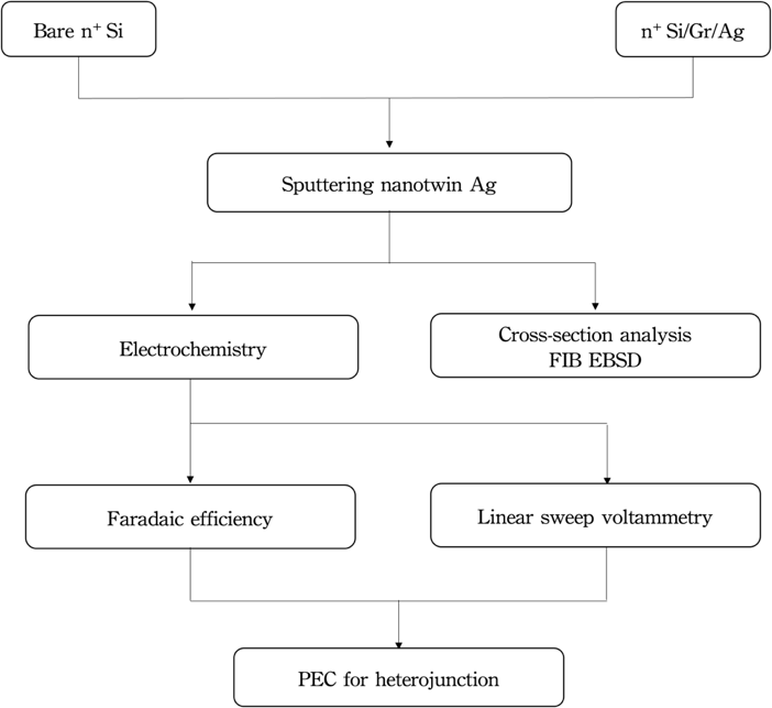
This experiment involves the fabrication of Si heterojunctions, followed by backside deposition, transfer of graphene layer, and deposition of silver thin film using magnetron sputtering. Figure 1 shows the schematic diagram of experimental procedure and analysis.
For the manufacturing of n+Si/graphene/ nanotwinned Ag photoelectrode, the Si substrates were ultrasonically cleaned in acetone and deionized water prior to the coating process to enhance the film's adhesion. A graphene layer was transferred on the Si substrate and then a nanotwinned Ag thin film was sputtered on the graphene deposited n+Si substrate. For comparison, the Ag film was also directly sputtered on a bare n+Si substrate without graphene layer.
To grow the graphene layer on Si substrate, chemical vapor deposition method was employed after electrochemical polishing of a copper foil. The copper foil was then placed into the quartz tube and load into the chamber. The chamber pressure was evacuated to 10-3 torr, and heated to 1000˚C for 40 minutes under the hydrogen flow with the flow rate of 10 sccm. Next, the copper foil was annealed at 1000˚C under hydrogen atmosphere (10 sccm) for an hour to reduce the oxidized copper and stimulate the grain growth, which can improve the quality of graphene. After annealing, insert the methane gas with the flow rate of 10 sccm and adjust the hydrogen gas to 100 sccm. At this stage, graphene is grown under the mixture of H2:CH4 =10:1 for an hour. Finally, CVD graphene is cooled down rapidly to the room-temperature under hydrogen atmosphere to avoide oxidize. Then the graphene layer would be transferred using a strong organic polymer, such as EVA, to tightly hold onto the graphene on the surface of a copper foil. Once the EVA has dried, the copper foil is placed in an etching solution (iron chloride, nitric acid) to remove the copper layer beneath the graphene. After etching, the remaining organic polymer and graphene film are cleaned with deionized water and placed onto the desired substrate. Using compressed air, the water underneath the graphene is blown away, allowing for van der Waals bonding between the graphene and the silicon substrate. Finally, the entire substrate is immersed in o-Xylene at 800C to remove the surface organic polymer layer, resulting in the successful transfer of graphene onto the desired substrate.
The thin nanotwinned silver films were produced using a DC magnetron sputtering system (JUBSUN TECH, SGS-500) in this study. The sputtering chamber was evacuated to a base pressure of <5×10⁻⁶ Torr, and high-purity (99.9995%) Argon gas was maintained at 5 mTorr (0.67 Pa). For the formation of nanotwinned structure, Ag thin films were deposited with sputtering power of 150 W and applied bias of -150V, and the deposition rate was 0.895 nm/s. The deposition temperature ranged from room temperature to 50°C, and the holder was fixed at 10 rpm. For the identification of Ag nanotwins, a focused ion beam (FIB, Hitachi NX2000) was used. Electron backscatter diffraction (EBSD) was conducted with JEOL JSM-7800F and analyzed in OIM TSL software to reveal the crystal orientations and twin densities of the films. The electrical resistivity is measured by Keithley 2401 source meter.
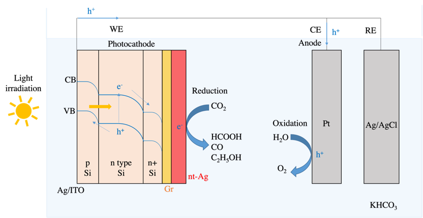
The schematic diagram of the PEC device is shown in Figure 2, consisting of three electrodes, including a photocathode composed of p-type Si, n-type Si, n+ Si, back electrode, graphene, and nanocrystalline silver thin film, forming a heterojunction. A three-electrode system allows for better control and measurement of current and potential, including a semiconductor photoelectrode (p-type or n-type), a metal-to-metal contact, and a reference electrode. The photoelectrode typically contains semiconductor materials, catalysts, and conductive materials. When the photoelectrode is irradiated by light and the energy of the light is greater than the band gap of the semiconductor material, a photoelectric effect occurs, and bound electrons are excited from the valence band to the conduction band, generating electron-hole pairs that undergo reduction or oxidation reactions on the surface of the material. The catalyst reduces the energy barrier for the reaction, and the conductive material is responsible for transmitting electrons and maintaining the electrochemical system's circuit. For an n-type semiconductor photoelectrode, holes are brought to the surface to undergo oxidation reactions, while electrons are transmitted to the counter electrode via an external circuit, where reduction reactions occur. The auxiliary electrode only serves to balance the charge and is usually made of platinum, which has high stability and conductivity to complete the electron circuit.
To evaluate the photoelectrochemical efficiency for the n+Si/graphene/ nanotwinned Ag photoelectrode, electrochemical Co2RR measurements were conducted, including Faraday efficiency and linear sweep voltammetry, followed by application in photoelectrochemical (PEC) and measurement of the catalytic effect. Graphene provides accelerated carrier transport, which can enhance the performance and stability of the device in electrolyte [9]. Thus, we compare the samples with and without graphene layer in this study.
The thickness of this transition layer was determined by measuring the distance from the Ag/Gr boundary to the deposition front of the grown Ag random grains at 10 equally-spaced points on the FIB micrograph and calculating the average thickness. The standard deviation for various transition layers was between 0.16 and 0.29 μm. In addition, the electron backscatter diffraction technique can be combined with OIM software to analyze the proportion of (111) crystal grain orientations, Σ3 coincident grain boundaries and grain size proportions in the nanotwin thin film. The calculation of coincident site lattice grain boundaries as a proportion of the total grain boundaries is set with a permissible tolerance angle of 15 degrees.
3. Results and Discussion
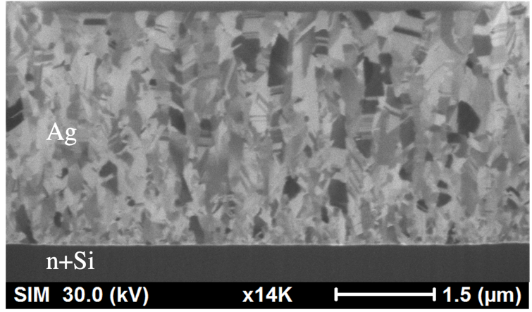
The Ag thin films were directly deposited onto n+Si substrates without transferred graphene in order to compare with the one with graphene layer. The cross-sectional microstructures of Ag films that were sputtered on bare n+Si substrates were shown in Figure 3. Certain nanotwins with parallel aligned twin boundaries can be found in the cross-section of the sputtered Ag thin film with an average transition layer of 2.1 μm. However, the twin density as evaluated in the Ag film is less than 30% as shown in Figure 3. In addition, the nanotwinned Ag film was found to have only minimal photoelectrochemical effect and is easy to peel off. In order to enhance the PEC reaction and the film adhesion, the other samples were sputtered after transferring a layer of graphene on the Si substrates. It is expected that, through the sandwiching of a graphene between the Si substrate and Ag nanotwinned film, the carrier transportation can be accelerated and the improvement of device stability and performance in electrolytes can be achieved. Furthermore, the strengthening effect of graphene for the Si/ Ag interface can prevent the peel-off phenomenon of the sputtered Ag nanotwinned film.
Thus, we transfer a graphene layer on the n+Si substrate. Figure 4a shows the optical microscopy image of transferred graphene layer on n+ Si substrate, and the Raman spectra of the graphene layer is shown in Figure 4b. It can be seen that the peak of G and 2D appeared obviously in the spectra, and the spectra shows that the sharp 2D peak, which means it has less defect and the graphene is monolayer. In addition, the ratio of intensity is about 1:2, indicating the graphene layer truly existed. Figure 5 indicates Raman mapping of graphene after sputtering of both G band and 2D band as shown in Figure 5 indicates that the graphene layer was maintained on the n+Si after sputtering and distributed quite uniform on the substrate.
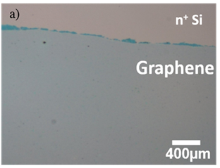
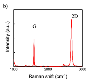
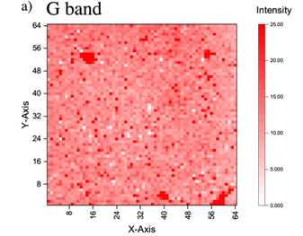
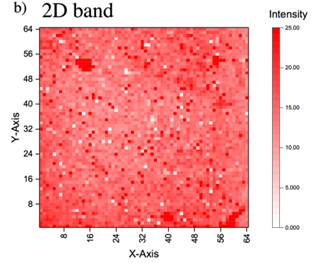
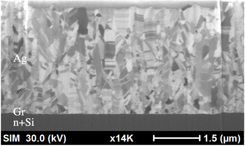
Figure 6 reveals the FIB images of Ag films that were deposited onto n+Si substrates with transferred graphene. The Ag films had also the thicknesses of 4μm. The micrographs reveal that Ag columnar grains grew normally to the Si substrate, and nanotwins piled up on one another. It can also be observed that the twin density in this Ag thin film sputtered on graphene deposited Si substrate is higher than that without graphene layer shown in Fig. 3. In addition, the average transition layer is about 1.4 μm, much finer than that in Fig.3.
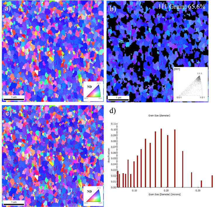
In order to clarify the grain orientations of the Ag thin films, EBSD analysis was showed in figure 7. The EBSD orientation map revealed that the silver films were highly oriented with high density of Ag (111) grains. The ratio of (111)-oriented grains in silver films were calculated to be over 65%, as shown in Figure 7b. In addition, the twin boundaries with Σ3 coincidence site lattice are highlighted with red lines in Figure 7c, with 21.2% of Σ3 boundaries to the total grain boundaries. Furthermore, the grain size in nanotwinned silver film was summarized in the bar chart, indicating that the silver grain sizes were in the range of several hundred nanometers.
The electrical resistivity of the Ag nanotwinned films on graphene transferred n+Si substrates was measured. The twin density increased after adding a transferred graphene layer in the device, and the electrical resistivity also decreased from 4.1*10-8 (Ω∙m) to 2.9*10-8 (Ω∙m), which enhances the electrical conduction. These results suggest that adding a graphene layer on Si substrates before sputtering process of Ag thin films has effectively promoted the formation of nanotwinned structure in the Ag films, and the results allow us to further reveal more facts about the performance of nanotwinned silver film of n+ Si/Gr/sputtered Ag structure.
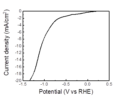
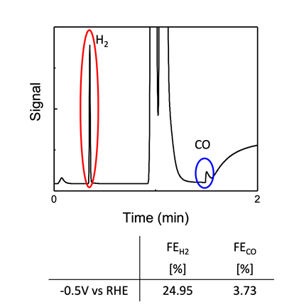
The catalysis of nanotwinned silver film in CO2RR is shown in Figure 8, and the onset potential@10mA/cm2 is -1.0V. Furthermore, Figure 9 reveals the gas chromatography curve of CO2RR products from nanotwinned silver film. It can be seen that there are two peaks of hydrogen and carbon monoxide, respectively. It has been calculated by calibration curve, the Faraday efficiency of hydrogen and carbon monoxide are 24.95% and 3.73%.
Here, graphene acts as the transparent electron to provide carrier transportation and as a passivation layer to prevent the electrolyte from destroying Si substrate, which can further improve the performance and stability of the electrochemical device and can also use in PEC to achieve the same effect. Plus, device with graphene layer can also increase the twin density and improve the film adhesion. The results evidenced that the n+ Si/Gr/nanotwinned Ag photoelectrode in this study has obvious Co2 reduction and hydrogen production effect. It is expected that the beneficial effect of nanotwinned structure in Ag films sputtered on graphene coated Si substrates can be amplified even more with the increase of twin density, which is achievable through the employment of an optimized bias voltage during the sputtering process as proposed by Chuang et al. [10].
Conclusions
In this study, the structure of n+ Si/Gr/sputtered Ag has been applied as the photoelectrode for photoelectrochemical Co2 reduction reaction. We successfully produced nanotwinned Ag films on graphene transferred n+Si substrates with DC magnetron sputtering process with applied bias. The addition of graphene layer was proved to increase the density of the nanotwins and improve the quality of the sputtered Ag thin films. In addition, the electrical resistivity also enhanced. Further, the catalysis of nanotwinned silver film in Co2RR indicated the onset potential@10mA/cm2 is -1.0V. Additionally, hydrogen and carbon monoxide are the main two products, and the production of hydrogen was higher, with the Faraday efficiency of hydrogen reaching 24.95%. Further improvement of the PEC Co2RR effect is expected through an optimized bias during the sputtering process to obtain a high twin density in the Ag films.
Acknowledgements
This study was sponsored by the Emerging Technology Application Program of the Hsinchu Science Park R & D program of Ag Materials Technology Co., LTD under Grant No. 112AO03A.
References
[1] T. Hatsukade, K. P. Kuhl, E. R. Cave, D. N. Abram, and T. F. Jaramillo, "Insights into the electrocatalytic reduction of Co2 on metallic silver surfaces," Phys. Chem. Chem. Phys., vol. 16, no. 27, pp. 13814-13819, 2014. View Article
[2] Xu, Y.; Li, C.; Xiao, Y.; Wu, C.; Li, Y.; Li, Y.; Han, J.; Liu, Q.; He, J, "Tuning the Selectivity of Liquid Products of Co2RR by Cu-Ag Alloying," ACS Appl Mater Interfaces, vol. 14, no. 9, pp. 11567-11574, Mar. 2022. View Article
[3] Chou, T.-C.; Chang, C.-C.; Yu, H.-L.; Yu, W.-Y.; Dong, C.-L.; Velasco-Vélez, J.-J.; Chuang, C.-H.; Chen, L.-C.; Lee, J.-F.; Chen, J.-M.; Wu, H.-L., "Controlling the Oxidation State of the Cu Electrode and Reaction Intermediates for Electrochemical Co2 Reduction to Ethylene," J Am Chem Soc, vol. 142, no. 6, pp. 2857-2867, Feb. 2020. View Article
[4] Tang, C.; Shi, J.; Bai, X.; Hu, A.; Xuan, N.; Yue, Y.; Ye, T.; Liu, B.; Li, P.; Zhuang, P.; Shen, J.; Liu, Y.; Sun, Z., "Co2 Reduction on Copper's Twin Boundary," ACS Catal, vol. 10, no. 3, pp. 2026-2032, Feb. 2020. View Article
[5] Hu, F.; Abeyweera, S. C.; Yu, J.; Zhang, D.; Wang, Y.; Yan, Q.; Sun, Y., "Quantifying Electrocatalytic Reduction of Co2 on Twin Boundaries," Chem, vol. 6, no. 11, pp. 3007-3021, 2020. View Article
[6] Tang, C.; Chen, Z.; Wang, Y.; Xiao, T.; Li, X.; Zheng, C.; Xu, X.; Sun, Z., "Atomic Editing Copper Twin Boundary for Precision Co2 Reduction," ACS Catal, pp. 11838-11844, Sep. 2022. View Article
[7] Cai, J.; Zhao, Q.; Hsu, W.-Y.; Choi, C.; Liu, Y.; Martirez, J. M. P.; Chen, C.; Huang, J.; Carter, E. A.; Huang, Y., "Highly Selective Electrochemical Reduction of Co2 into Methane on Nanotwinned Cu," J Am Chem Soc, vol. 145, no. 16, pp. 9136-9143, Apr. 2023. View Article
[8] T.-H. Chuang, P.-C. Wu, and Y.-C. Lin, "Lattice buffer effect of Ti film on the epitaxial growth of Ag nanotwins on Si substrates with various orientations," Mater Charact, vol. 167, p. 110509, 2020. View Article
[9] Ku, C.-K.; Wu, P.-H.; Chung, C.-C.; Chen, C.-C.; Tsai, K.-J.; Chen, H.-M.; Chang, Y.-C.; Chuang, C.-H.; Wei, C.-Y.; Wen, C.-Y.; Lin, T.-Y.; Chen, H.-L.; Wang, Y.-S.; Lee, Z.-Y.; Chang, J.-R.; Luo, C.-W.; Wang, D.-Y.; Hwang, B. J.; Chen, C.-W., "Creation of 3D Textured Graphene/Si Schottky Junction Photocathode for Enhanced Photo-Electrochemical Efficiency and Stability," Adv Energy Mater, vol. 9, no. 29, p. 1901022, Aug. 2019. View Article
[10] P.-C. Wu, Y.-C. Lai, and T.-H. Chuang, “Enhancing effect of substrate bias on nanotwin formation of sputtered Ag thin films,” Journal of Materials Science: Materials in Electronics, vol. 32, no. 17, pp. 21966–21973, 2021. View Article