International Journal of Mining, Materials, and Metallurgical Engineering (IJMMME)
ISSN: 2562-4571

Volume 10 - Year 2024 - Pages 1-7
DOI: 10.11159.ijmmme.2024.001
Ultra-Thin Cu Nano-Twinned Films Sputtered On Si Wafers for Low Temperature Hybrid Bonding Of Advanced 3D-IC Packages
Zi-Hong Yang1, Yen-Ting Chen2, Yin-Hsuan Chen2, and Tung-Han Chuang*3
1Taiwan Semiconductor Manufacturing Co., TSMC, Hsinchu Science Park, Hsinchu 30078, Taiwan.
2 Institute of Materials Science and Engineering, National Taiwan University, Taipei 106, Taiwan.
3Ag Materials Technology Co., LTD, Hsinchu Science Park, Hsinchu 30078, Taiwan.
johnson86115@gmail.com ; a5331812@gmail.com ; sammichen8815@gmail.com ; tunghan@ntu.edu.tw
*Corresponding author: tunghan@ntu.edu.tw
Abstract - The nanotwinned structure has been attracting a great deal of attention due to its excellent mechanical and electrical properties. In this study, ultra-thin nanotwinned Cu (nt-Cu) films with a thickness of 1.5 μm were fabricated by DC magnetron sputtering with moderate substrate bias. Within these films, an equiaxed-grain transition layer only 100–400 nm thick formed between the nanotwinned region and Si substrate and was observed by focused ion beam (FIB). The XRD and EBSD analyses indicated that the as-deposited nanotwinned films had a strong (111) preferred orientation. The surface roughness of the films, as measured with an atomic force microscope (AFM), was below 10 nm, which was sufficiently smooth for chip bonding at low temperature with minor pressure. Direct bonding of Si chips sputtered with such ultra-thin nt-Cu films with a (111) preferred orientation has been evidenced to yield a sound interface, and this bonding method can be applied for the manufacturing of 3D-IC packages.
Keywords: Cu Nanotwin, Hybrid Bonding, 3D-IC Packages
© Copyright 2024 Authors This is an Open Access article published under the Creative Commons Attribution License terms. Unrestricted use, distribution, and reproduction in any medium are permitted, provided the original work is properly cited.
Date Received: 2023-04-07
Date Revised: 2024-01-18
Date Accepted: 2024-01-26
Date Published: 2024-02-28
1. Introduction
Nowadays, the three-dimensional integrated circuit (3D-IC) is a novel structure that plays a key role in advanced packaging technology, which focuses on downscaling device packages, reducing the thermal budget, and enhancing the mechanical reliability and electrical properties [1-4]. Through 3D chip stacking, it is possible to extend the number of functions per 3D chip well beyond the capabilities of traditional scaling. 3D stack interconnections can be achieved either by copper-to-copper direct bonding or solder bonding. Among these methods, Cu–Cu direct bonding is more promising for fine-pitch high-density interconnections because of the low melting point of tin (Sn). At a reflow temperature above the melting point of Sn, the molten solder may spread and join together, which can cause shorting when the pitch is below 20 μm [5]. In addition, if Cu–Cu bonding is used in through silicon via (TSV) 3D stacking, the TSV and the bonding joint both consist of pure copper and thus have the same physical and electrical properties. Cu is also lower in cost than solder. As a result, Cu–Cu direct bonding is a potential method for bonding and appears to be the most promising solution for exceeding the physical limit of Moore’s Law.
Traditionally, direct Cu–Cu bonding can be achieved by thermal compression at temperatures of 300 °C for more than 30 min [6-8], but because of the high temperature, reliability issues may arise. Thus, low temperature Cu–Cu bonding (< 250°C) is gaining interest. Kim et al. reported that Cu–Cu direct bonding at the wafer level was performed at room temperature by surface activated bonding (SAB) with a low energy Ar ion beam under ultra-high vacuum (UHV) conditions [9]. However, this process is rather time-consuming and expensive. Nanotwinned copper has been reported to have distinctive properties, such as high surface diffusivity and good mechanical and electrical properties [10-14]. Chen et al. has reported that low-temperature (150°C) and low-pressure (114 psi) Cu–Cu direct bonding can be performed in ordinary vacuum by using (111)-oriented nt-Cu films obtained by electroplating [15]. The reason is that Cu has a face-centred cubic structure, and (111), the closest packed plane, possesses the highest diffusivity among all the planes in Cu. The diffusivity on the (111) surface of Cu is at least 30,000 times greater than that on low-index planes such as (100) and (110) [16-18]. In addition, the oxidation rate of (111)-oriented nanotwinned Cu is the lowest [19]. Thus, the bonding can be performed rapidly if both Cu pieces are (111)-oriented and nanotwinned in structure. In addition to Cu–Cu direct bonding, other metal direct bonding methods have also been reported. It is reported that low temperature Ag–Ag direct bonding was achieved at 150–250 °C in 10–60 min in ordinary vacuum by using high (111)-preferred orientation films with densely-packed nanotwins fabricated by magnetron sputtering [20]. Chang et al. also used highly (111)-oriented nanotwinned Ag films to achieve metal bonding in 3 min in air atmosphere at 190/200 °C [21]. Wu et al. reported that highly (111)-oriented nanotwinned gold can be fabricated by periodically-reversed electroplating. Grain growth was observed to eliminate the bonding interface of the two films after annealing at 250 °C for 1h [22].
The above studies all used highly (111)-oriented nanotwinned films to achieve direct bonding of metals. Thus, the fabrication of high-quality, thin nanotwinned films has become an important issue. The nanotwinned film can be divided into two regions between the bottom substrate and the top surface. A columnar crystal region containing high density nanotwins grows near the surface. A randomly oriented equiaxed-grain region called the transition layer forms between the substrate and the nanotwinned region. The existence of the transition layer is caused by the lattice mismatch of the nanotwinned region and the substrate. For the electrodeposition of (111)-oriented Cu nanotwinned films, a strong (111)-oriented Cu seed layer formed by sputtering is needed. The seed layer can effectively reduce the thickness of the transition layer, which consists of randomly-oriented fine grains that grow from the substrate, and this layer plays a crucial role in the regularity of (111)-oriented nanotwinned Cu [23]. Chen et al. reported that applying a reverse current can significantly suppress the formation of the transition layer, indicating that the reverse current may remove or retard the growth of these grains [24]. Kim et al. also reported that the reverse current has a selective dissolution behavior that causes non-(111)-oriented grains to be dissolved earlier due to their higher surface energy than that of (111)-oriented grains, which facilitates the formation of the columnar nanotwinned Cu microstructure [25]. Chuang et al. reported that a (002) Ti adhesive layer not only enhances the bonding strength between a metallic film and Si substrate but also alleviates the lattice mismatch, allowing the epitaxial growth of nanotwinned Ag films on Si substrates, which in turn decreases the thickness of the transition layer [26]. Lai also reported that a thicker transition layer tends to have poorer thermal stability due to the tendency of grain growth of the random grains to replace the Ag nanotwinned structure, especially at high temperatures [27]. The above studies aimed to decrease the thickness of the transition layer and optimize high-density nanotwinned films with a strong (111) surface orientation, but few studies have considered the optimization of nanotwinned films in the sputtering process. In this study, substrate bias was applied to reduce the thickness of the transition layer with the Ar+ ion bombardment effect. With moderate substrate bias, ultra-thin Cu nanotwinned films with a strong (111) surface orientation can be fabricated for metal-to-metal direct bonding applications such as 3D-IC advance packages. The effect of bias-induced ion bombardment on the deposition of ultra-thin nanotwinned films is also discussed.
2. Experimental
For the experiments, Cu nanotwinned thin films with a thickness of 1.5 μm were deposited on Si chips in a DC magnetron sputtering system (JUBSUN TECH, SGS-500) with a base pressure of < 5×10^(-6) Torr (6×10^(-4) Pa). Prior to the deposition process, the Si substrates were properly cleaned with acetone, ethanol and deionized water to promote adhesion of the films, and the substrate was pre-sputtered by argon discharge at a bias of -500 V for 30 min to remove the surface oxide layer. For the sputtering process, argon gas was used as the working gas, with the pressure maintained at 5 mTorr (0.67 Pa), and the rotation speed of the holder was 10 rpm. The sputtering powers of Ti and Cu were 150 W, and the deposition rates were 0.1 nm/s and 0.35 nm/s, respectively. Ti was pre-coated on the Si substrate as an adhesive layer to promote adhesion between the thin film and the substrate. Various negative substrate biases were applied to induce Ar ion bombardment of the film surface during deposition. After the deposition, the samples were left in the chamber to cool to room temperature.
For metallographic observations, a focused ion beam (FIB, Hitachi NX2000) was employed to analyse the microstructure of the thin films and to prepare specimens for transmission electron microscopy (TEM, FEI Tecnai G2 F20). Film thickness was determined by FIB examination of cross-section images. The crystal orientations of the thin films were identified by X-ray diffraction (XRD, Rigaku TTRAX). The EBSD measurements were performed with a JEOL JSM-7800F and Orientation Imaging Microscopy (OIM) software (TSL, USA) to analyse the orientation maps, crystallographic textures and grain boundaries according to Kikuchi patterns. The surface roughness (Ra) values of the thin film surfaces were determined with an atomic force microscope (AFM, Burker Dimension Edge). Transmission electron microscopy (TEM, FEI Tecnai G2 F20) was used to analyse the arrangement of the nanotwins in columnar grains.
The measurement of the transition layer thickness entailed assessing the distance from the Cu/Ti boundary to the deposition front of the grown Cu random grains at ten evenly spaced points on the FIB micrograph. Subsequently, the average thickness was calculated. The standard deviation for the different transition layers varied between 0.12 and 0.25 μm.
3. Results and Discussions
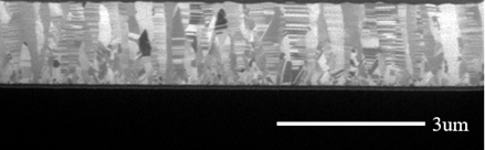
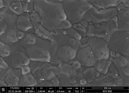
The cross-sectional FIB ion image in Figure 1 shows that the grain structure of the sputtered Cu thin film grew to 1.5 um with -150 V substrate bias. It can be seen that densely-packed nanotwins grew perpendicular to the substrate. The transition layer, where the equiaxed Cu grains had random orientations, was calculated to be 300 nm, indicating that the negative substrate bias voltage suppressed the bottom random grain structures and promoted the formation of a nanotwinned columnar grain structure. A plane view SEM image of the copper film surface is shown in Figure 2. This top view projection of the columnar grains shows numerous cone-shaped grains on the Cu film surface.
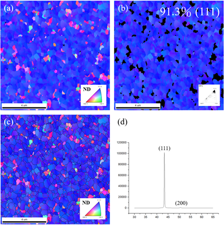
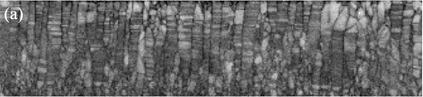
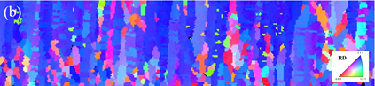
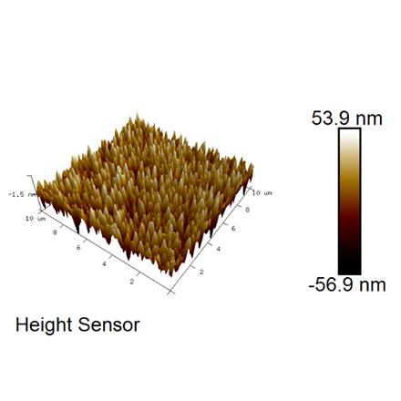
EBSD was employed to verify the grain orientations of the Cu films deposited with -150 V substrate bias. As shown in Figure 3, the EBSD orientation map of the Cu films indicated that the Cu grains were highly oriented in the (111) direction, and the proportions of the (111)-oriented grains were calculated to be 91.3%. In Figure 3c, the conventional grain boundaries are indicated by black lines, and the Σ3 coincident twin boundaries are marked with red lines. The proportion of Σ3 coincident twin boundaries to the total grain boundaries was 27.9%. Figure 3d shows the corresponding X-ray diffraction pattern with a strong (111) peak, indicating that these nanotwinned Cu films had a (111) preferred orientation. Figure 4a clearly shows the contrast of the nanotwinned structure, and Figure 4b presents a rolling-direction (RD) orientation image map of the sputtered Cu film. Grains at the bottom of the film appeared to be randomly oriented, and the grains above the transition layer were (111)-oriented. The surface topography was analysed by AFM, and the surface roughness (Ra) value was measured to be 8.5 nm.
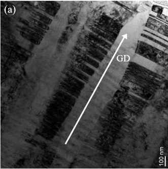
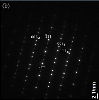
The microstructures of the Cu films were further analysed by transmission electron microscopy (TEM). A cross-sectional TEM bright field image of a nanotwinned Cu film deposited with -150 V substrate bias is shown in Figure 6a. The distribution of nanotwins and matrix in columnar grains was clearly observable in the bright-field TEM image of an integral nanotwinned columnar grain, and the growth direction of the Cu nanotwins was perpendicular to the substrate, as illustrated by the white arrow in Figure 6a. Figure 6b presents a selected area diffraction (SAD) pattern taken along the [110] zone axis, showing two sets of distinguished diffraction spots of matrix (M) and twins (T), which were symmetrical along the (11 ̅1 ̅)/(1 ̅11) co-plane, demonstrating the characteristic of a twin structure.The microstructures of the Cu films were further analysed by transmission electron microscopy (TEM). A cross-sectional TEM bright field image of a nanotwinned Cu film deposited with -150 V substrate bias is shown in Figure 6a. The distribution of nanotwins and matrix in columnar grains was clearly observable in the bright-field TEM image of an integral nanotwinned columnar grain, and the growth direction of the Cu nanotwins was perpendicular to the substrate, as illustrated by the white arrow in Figure 6a. Figure 6b presents a selected area diffraction (SAD) pattern taken along the [110] zone axis, showing two sets of distinguished diffraction spots of matrix (M) and twins (T), which were symmetrical along the (1![]() )/(
)/(![]() 11) co-plane, demonstrating the characteristic of a twin structure.
11) co-plane, demonstrating the characteristic of a twin structure.
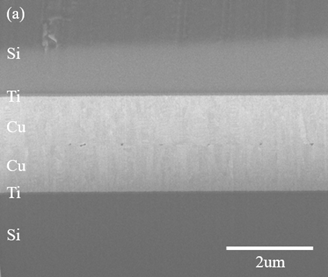
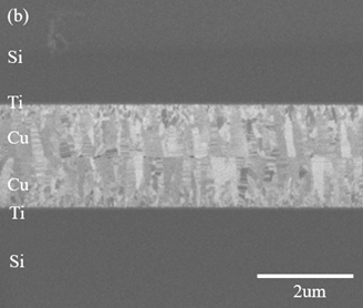
Direct metal bonding is promising because it has the potential to replace solder joints in packaging technology. Figure 7 presents cross-sectional FIB electron beam and ion beam images on the bonding results of two (111)-oriented nt-Cu films at 200 °C for 60 min under 20 Mpa in a regular vacuum of 1×10^(-3) torr. The results showed that the bonding interface had only a few small voids and no obvious grain growth. The primary capability of the low-temperature bonding behavior is attributed to the presence of the (111)-oriented FCC metal surface, such as those of Ag and Cu, which possesses the highest surface diffusivity values among all the crystallographic planes. In addition, the oxidation rate of the Cu (111) surface is the slowest relative to those of the other planes. Therefore, 3D-IC bonding can be performed rapidly if both bonding metals are (111) oriented and nanotwinned in structure.
4. Conclusions
In summary, ultra-thin Cu nanotwinned films with a thickness near the submicron scale and a strong (111) orientation were successfully fabricated by using DC magnetron sputtering with moderate substrate bias. According to the characterization of the cross-sectional microstructure, an equiaxed-grain transition layer only 100–400 nm thick was observed between the nanotwinned region and Si substrate. The results showed that the thickness of the transition layer can be effectively reduced by the Ar+ ion bombardment effect, indicating that high-quality nanotwinned films can be fabricated at a thinner thickness. The nanotwinned films in our work were shown to have a strong (111) preferred orientation, and the surface roughness was sufficiently smooth to achieve metal-to-metal direct bonding. These ultra-thin nt-Cu films with (111) preferred orientation are potentially applicable to the direct bonding of advanced chip-on-wafer (CoW) or wafer-on-wafer (WoW) 3D-IC packages.
Acknowledgement
This study was sponsored by the Emerging Technology Application Program of the Hsinchu Science Park R & D program of Ag Materials Technology Co., LTD under Grant No. 112AO03A.
References
[1] Madden, L., Wu, E., Kim, N., Banijamali, B., Abugharbieh, K., Ramalingam, S., & Wu, X. (2012, September). Advancing high performance heterogeneous integration through die stacking. In 2012 Proceedings of the European Solid-State Device Research Conference (ESSDERC) (pp. 18-24). IEEE. View Article
[2] Alam, A., Hanna, A., Irwin, R., Ezhilarasu, G., Boo, H., and Iyer, S. S. (2019, May). Heterogeneous integration of a fan-out wafer-level packaging based foldable display on elastomeric substrate. In 2019 IEEE 69th Electronic Components and Technology Conference (ECTC) (pp. 277-282). IEEE. View Article
[3] Chiu, W. L., Liu, C. M., Haung, Y. S., & Chen, C. (2014). Formation of nearly void-free Cu3Sn intermetallic joints using nanotwinned Cu metallization. Applied Physics Letters, 104(17), 171902. View Article
[4] Chang, Y. W., Liang, S. W., & Chen, C. (2006). Study of void formation due to electromigration in flip-chip solder joints using Kelvin bump probes. Applied physics letters, 89(3), 032103. View Article
[5] Liu, Y., Lu, Y., & Tu, K. N. (2022). Low temperature interfacial reaction in 3D IC nanoscale materials. Materials Science and Engineering: R: Reports, 151, 100701. View Article
[6] Tan, C. S., Peng, L., Fan, J., Li, H., & Gao, S. (2012). Three-dimensional wafer stacking using Cu-Cu bonding for simultaneous formation of electrical, mechanical, and hermetic bonds. IEEE Transactions on Device and Materials Reliability, 12(2), 194-200. View Article
[7] Lee, J., Fernandez, D. M., Paing, M., Yeo, Y. C., & Gao, S. (2012). Electroless Ni plating to compensate for bump height variation in Cu-Cu 3-D packaging. IEEE Transactions on Components, Packaging and Manufacturing Technology, 2(6), 964-970. View Article
[8] Chen, K. N., Lee, S. H., Andry, P. S., Tsang, C. K., Topol, A. W., Lin, Y. M., ... & Haensch, W. (2006). International Electron Devices Meeting (IEDM). San Francisco CA.
[9] Kim, T. H., Howlader, M. M. R., Itoh, T., & Suga, T. (2003). Room temperature Cu-Cu direct bonding using surface activated bonding method. Journal of Vacuum Science & Technology A: Vacuum, Surfaces, and Films, 21(2), 449-453. View Article
[10] Z. Cheng, H. Zhou , Q. Lu , H. Gao , L. Lu , Extra strengthening and work hardening in gradient nanotwinned metals, Science 362 (6414) (2018) 1925. View Article
[11] B. Z. Cui, K. Han, Y. Xin, D.R. Waryoba, A.L. Mbaruku, Highly textured and twinned Cu films fabricated by pulsed electrodeposition, Acta Mater. 55 (2007) 4 429-4 438. View Article
[12] Z. S. You, L.Lu, K. Lu, Tensile behavior of columnar grained Cu with preferen- tially oriented nanoscale twins, Acta Mater. 59 (2011) 6927-6937. View Article
[13] O. Anderoglu, A. Misra, H. Wang, F. Ronning, M. F. Hundley, X. Zhang, Epitaxial nanotwinned Cu films with high strength and high conductivity, Appl. Phys. Lett. 93 (8) (2008) 083108. View Article
[14] L. Lu, Y. Shen, X. Chen, L. Qian, K. Lu, Ultrahigh strength and high electrical conductivity in copper, Science 304 (5669) (2004) 422-426. View Article
[15] Chen, C., Liu, C. M., Lin, H. W., Huang, Y. S., Chu, Y. C., Lyu, D. R., ... & Tu, K. N. (2016, January). Low-temperature and low-pressure direct copper-to-copper bonding by highly (111)-oriented nanotwinned Cu. In 2016 Pan Pacific Microelectronics Symposium (Pan Pacific) (pp. 1-5). IEEE. View Article
[16] Butrymowicz, D. B., Manning, J. R., & Read, M. E. (1973). Diffusion in copper and copper alloys. Part I. volume and surface self‐diffusion in copper. Journal of Physical and Chemical Reference Data, 2(3), 643-656. View Article
[17] Agrawal, P. M., Rice, B. M., & Thompson, D. L. (2002). Predicting trends in rate parameters for self-diffusion on FCC metal surfaces. Surface Science, 515(1), 21-35. View Article
[18] Liao, C. N., Lu, Y. C., & Xu, D. (2013). Modulation of crystallographic texture and twinning structure of Cu nanowires by electrodeposition. Journal of the Electrochemical Society, 160(6), D207. View Article
[19] Zhou, G., & Yang, J. C. (2005). Initial oxidation kinetics of Cu (100),(110), and (111) thin films investigated by in situ ultra-high-vacuum transmission electron microscopy. Journal of Materials Research, 20(7), 1684-1694. View Article
[20] Lai, Y. C., Wu, P. C., & Chuang, T. H. (2021). Characterization of interfacial structure for low-temperature direct bonding of Si substrates sputtered with Ag nanotwinned films. Materials Characterization, 175, 111060. View Article
[20] Zhan, X., Lian, J., Li, H., Wang, X., Zhou, J., Trieu, K., & Zhang, X. "Preparation of highly (111) textured nanotwinned copper by medium-frequency pulsed electrodeposition in an additive-free electrolyte." Electrochimica Acta 365 (2021): 137391. View Article
[21] Chang, L. P., Wang, J. J., Hung, T. H., Chen, K. N., & Ouyang, F. Y. (2022). Direct metal bonding using nanotwinned Ag films with (1 1 1) surface orientation under air atmosphere for heterogeneous integration. Applied Surface Science, 576, 151845. View Article
[22] Wu, J. A., Huang, C. Y., Wu, W. W., & Chen, C. (2018). Fabrication of (111)-oriented nanotwinned Au films for Au-to-Au direct bonding. Materials, 11(11), 2287. View Article
[23] Liu, C. M., Lin, H. W., Lu, C. L., & Chen, C. (2014). Effect of grain orientations of Cu seed layers on the growth of< 111>-oriented nanotwinned Cu. Scientific reports, 4(1), 1-4. View Article
[24] Chen, K. J., Wu, J. A., & Chen, C. (2020). Effect of Reverse Currents during Electroplating on the⟨ 111⟩-Oriented and Nanotwinned Columnar Grain Growth of Copper Films. Crystal Growth & Design, 20(6), 3834-3841. View Article
[25] Kim, M. J., Lim, T., Park, K. J., Cho, S. K., Kim, S. K., & Kim, J. J. (2012). Characteristics of pulse-reverse electrodeposited Cu thin films: I. effects of the anodic step in the absence of an organic additive. Journal of The Electrochemical Society, 159(9), D538. View Article
[26] Chuang, T. H., Wu, P. C., & Lin, Y. C. (2020). Lattice buffer effect of Ti film on the epitaxial growth of Ag nanotwins on Si substrates with various orientations. Materials Characterization, 167, 110509. View Article
[27] Lai, Y. C., Wu, P. C., & Chuang, T. H. (2021). Thermal stability of grain structure for Ag nanotwinned films sputtered with substrate bias. Materialia, 20, 101215. View Article